-31-
1
2
3
4
5
6
7-9
10-15
16
17
18
19
20
21
22
23-29
30-36
37
38
39
40
41
42
43
44-46
47
48
49
50-52
53
54
55
56-58
59
60
61
62-64
65
66
67
68
Pin No.
Pin Name
I/O
Description
IC DESCRIPTION-4/7 (CL680)-1/3
NC
VSS
CD BCK
CD DATA
CD LRCK
CD C2PO
NC
MD0-MD5
VSS
MD6
VDD3
MD7
VSS
MD8
VDD3
MD9-MD15
NC
________
MCE
__________
MWE
VSS
________
CAS
VDD3
___________
RASO
___________
RASI
MA10-MA8
VSS
MA7
VDD3
MA6-MA4
VSS
MA3
VDD3
MA2-MA0
PGIO7
______________
RESET
VDD MAX IN
NC
AGND DAC
A DAC
COMP OUT
AGND DAC
—
—
I
I
I
I
—
I/O
—
I/O
—
I/O
—
I/O
—
I/O
—
—
O
—
O
—
O
O
O
—
O
—
O
—
O
—
O
I/O
I
—
—
—
—
O
—
No connection.
GND.
Bit clock input from CD DSP.
Data input from CD DSP.
LRCK input from CD DSP.
C2 pointer input from CD DSP.
No connection.
DRAM/ROM interface. (DATA)
Ground.
DRAM/ROM interface. (DATA)
Power supply 3.3V.
DRAM/ROM interface. (DATA)
Ground.
DRAM/ROM interface. (DATA)
Power supply 3.3V.
DRAM/ROM interface. (DATA)
No connection.
ROM chip enable.
DRAM write enable.
Ground.
DRAM/ROM interface.
Power supply 3.3V.
DRAM/ROM interface. (Pin 43 is no connection)
DRAM/ROM interface. (Address)
Ground.
DRAM/ROM interface. (Address)
Power supply 3.3V.
DRAM/ROM interface. (Address)
Ground.
DRAM/ROM interface. (Address)
Power supply 3.3V.
DRAM/ROM interface. (Address)
Programmable I/O. (No connection)
Reset input.
Power supply - VDDMAX. (5.0V)
No connection.
Analog ground.
Analog power supply (DAC) : 3.3V.
Composite out.
Analog ground.
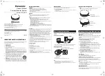
Summary of Contents for LCX-K277
Page 2: ... 2 SPECIFICATIONS Design and specifications are subject to change without notice ...
Page 11: ... 11 SCHEMATIC DIAGRAM 2 5 MAIN2 2 TUNER C700 0 1 12V ...
Page 16: ... 16 SCHEMATIC DIAGRAM 4 5 VCD1 2 PIN3 R140 5 6k C320 0 1 FZ ...
Page 17: ... 17 SCHEMATIC DIAGRAM 5 5 VCD2 2 J501 ...
Page 20: ... 20 VOLTAGE CHART 1 1 ...
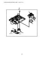
Page 44: ... 44 CD MECHANISM EXPLODED VIEW 1 1 DTA11T3C A M2 PIN 3 SW1 MOTOR C B 4 3 2 1 ...


