background image

– 16 –

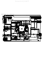
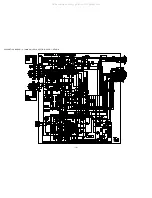
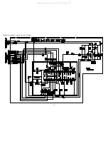
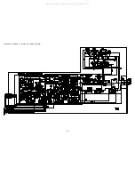
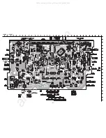
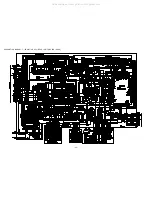
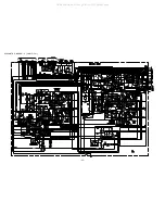
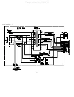
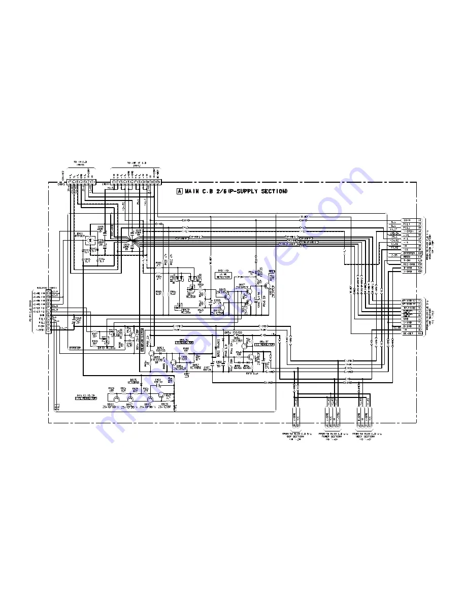
SCHEMATIC  DIAGRAM – 2  (MAIN 2/6) <P-SUPPLY SECTION>

All manuals and user guides at all-guides.com

all-guides.com

Summary of Contents for NSX-T929

Page 1: ...G 1 ZZRNDM NSX T929 LH S M Code No 09 013 440 2R1 This Service Manual is the Revision Publishing and replaces Simple Manual of NSX T929 LH S M Code No 09 00C 440 2T1 If requiring information about the...

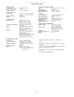
Page 2: ...em AC bias Heads Deck 1 Playback head x 1 Deck 2 Recording playback head x 1 erase head x 1 Compact disc player section Laser Semiconductor laser 780 nm D A converter 1 bit dual Signal to noise ratio...

Page 3: ...s tt n vad som specificeras i denna bruksanvising kan anv ndaren uts ttas f r osynling laserstr lning som verskrider gr nsen f r laserklass 1 PROTECTION OF EYES FROM LASER BEAM DURING SERVICING CAUTI...

Page 4: ...m that the main power is turned on and the HOLD terminal of the MICROCOMPUTER keeps the H level or not 3 3 3 3 3 When the HOLD terminal is L level the abnormality detection circuit is judged to be wor...

Page 5: ...c capacitor C113 that is connected to VDD of the MICROCOMPUTER with tweezers 3 3 3 3 3 Connect the AC power cord again If the MICROCOMPUTER returns to the normal operation the MICROCOMPUTER is good No...

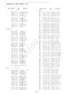
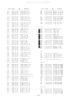
Page 6: ...VR C20 87 016 035 090 CAP E 6800 35 VR C31 87 A12 062 080 CAP E 100 10 SMG C32 87 012 286 080 C CAP U 0 01 25 K B C33 87 A12 071 080 CAP E 47 25 SMG C34 87 A12 089 080 CAP E 3 3 50 SMG C35 87 012 286...

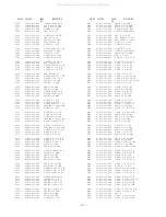
Page 7: ...80 CAP E 10 50 SMG C641 87 A12 087 080 CAP E 1 50 SMG C642 87 A12 087 080 CAP E 1 50 SMG C643 87 010 831 080 C CAP U 0 1 16F C644 87 A12 087 080 CAP E 1 50 SMG C645 87 A12 088 080 CAP E 2 2 50 SMG C64...

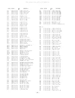
Page 8: ...LT2J R104 87 A01 002 050 RES 270 1 2W J BLT2J R790 87 012 286 080 C CAP U 0 01 25 B R991 87 012 195 080 C CAP U 100P 50CH R993 87 012 195 080 C CAP U 100P 50CH R995 87 012 195 080 C CAP U 100P 50CH SF...

Page 9: ...EVQ11G04M S222 87 A90 095 080 SW TACT EVQ11G04M S223 87 A90 095 080 SW TACT EVQ11G04M S224 87 A90 095 080 SW TACT EVQ11G04M S225 87 A90 095 080 SW TACT EVQ11G04M S226 87 A90 095 080 SW TACT EVQ11G04M...

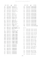
Page 10: ...7 A00 669 080 RES M F 0 22 2W J RA R161 87 A00 669 080 RES M F 0 22 2W J RA R162 87 A00 669 080 RES M F 0 22 2W J RA R163 87 A00 669 080 RES M F 0 22 2W J RA R164 87 A00 669 080 RES M F 0 22 2W J RA R...

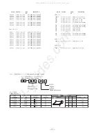
Page 11: ...NGE LED440 87 A41 055 040 LED HLMF K405 ORANGE DESCRIPTION REF NO KANRI NO PART NO 8 8 A Resistor Code Chip Resistor Part Coding Figure Value of resistor Chip resistor Wattage Type Tolerance 1 16W 1 1...

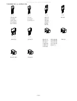
Page 12: ...SA1981Y 2SA1979O Y B C E 2SB1370 2SB1375 2SB1649 2SD2562 FN1016 FP1016 2SA1235F 2SC2714O 2SC3052F CMBT5401 CMBT5551 CSD1306E DTA114EKA DTA144EKA DTA143EKA DTC114EKA KRA107S B C E E C B 2SB1237Q G D S...

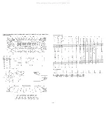
Page 13: ...13 FL HNA 13LM01 BNF4 GRID ASSIGNMENT ANODE CONNECTION PIN CONNECTION GRID ASSIGNMENT ANODE CONNECTION PIN CONNECTION All manuals and user guides at all guides com...

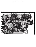
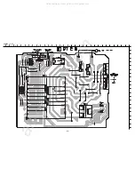
Page 14: ...WIRING 1 MAIN 32 31 30 29 28 27 26 25 24 23 22 21 20 19 18 17 16 15 14 13 12 11 10 9 8 7 6 5 4 3 2 1 14 A B C D E F G H I J K L M N O P Q R S T U All manuals and user guides at all guides com...
Page 15: ...15 SCHEMATIC DIAGRAM 1 MAIN 1 6 FUNCTION SECTION All manuals and user guides at all guides com...
Page 16: ...16 SCHEMATIC DIAGRAM 2 MAIN 2 6 P SUPPLY SECTION All manuals and user guides at all guides com a l l g u i d e s c o m...

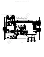
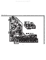
Page 17: ...17 SCHEMATIC DIAGRAM 3 MAIN 3 6 AMP SECTION All manuals and user guides at all guides com...

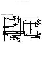
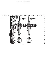
Page 18: ...18 SCHEMATIC DIAGRAM 4 MAIN 4 6 DECK SECTION HEAD 1 HEAD 2 All manuals and user guides at all guides com...

Page 19: ...19 SCHEMATIC DIAGRAM 5 MAIN 5 6 DSP SECTION All manuals and user guides at all guides com...

Page 20: ...20 SCHEMATIC DIAGRAM 6 MAIN 6 6 TUNER SECTION All manuals and user guides at all guides com...

Page 21: ...FRONT 32 31 30 29 28 27 26 25 24 23 22 21 20 19 18 17 16 15 14 13 12 11 10 9 8 7 6 5 4 3 2 1 21 A B C D E F G H I J K L M N O P Q R S T U All manuals and user guides at all guides com a l l g u i d e...

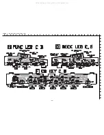
Page 22: ...3 CD KEY DECK LED FUNC LED 32 31 30 29 28 27 26 25 24 23 22 21 20 19 18 17 16 15 14 13 12 11 10 9 8 7 6 5 4 3 2 1 22 A B C D E F G H I J K L M N O P Q R S T U All manuals and user guides at all guide...

Page 23: ...23 SCHEMATIC DIAGRAM 7 FRONT CD KEY DECK LED FUNC LED DECK All manuals and user guides at all guides com...

Page 24: ...WIRING 4 AMP 1F VM 32 31 30 29 28 27 26 25 24 23 22 21 20 19 18 17 16 15 14 13 12 11 10 9 8 7 6 5 4 3 2 1 24 A B C D E F G H I J K L M N O P Q R S T U All manuals and user guides at all guides com...

Page 25: ...25 SCHEMATIC DIAGRAM 8 AMP 1F VM All manuals and user guides at all guides com...

Page 26: ...5 PT 32 31 30 29 28 27 26 25 24 23 22 21 20 19 18 17 16 15 14 13 12 11 10 9 8 7 6 5 4 3 2 1 26 A B C D E F G H I J K L M N O P Q R S T U All manuals and user guides at all guides com a l l g u i d e s...

Page 27: ...27 SCHEMATIC DIAGRAM 9 PT All manuals and user guides at all guides com...

Page 28: ...WIRING 6 DECK 32 31 30 29 28 27 26 25 24 23 22 21 20 19 18 17 16 15 14 13 12 11 10 9 8 7 6 5 4 3 2 1 28 A B C D E F G H I J K L M N O P Q R S T U All manuals and user guides at all guides com...

Page 29: ...29 IC BLOCK DIAGRAM All manuals and user guides at all guides com...

Page 30: ...30 All manuals and user guides at all guides com...

Page 31: ...31 All manuals and user guides at all guides com a l l g u i d e s c o m...

Page 32: ...nalyzer IC AD input output L at HOLD 23 I CDSW I CD mecha switches AD input output L at HOLD 24 I DISH I CD turnable sensor input output L at HOLD 25 I MIC I MIC input for auto vocal fader output L at...

Page 33: ...t output 75 CAM1 P10 I O Deck 1 CAM switch input FL P10 segment output 76 AUTO2 P9 I O Deck 2 auto stop input FL P9 segment output 77 AUTO1 P8 I O Deck 1 auto stop input FL P8 segment output 78 CAM2 P...

Page 34: ...n SFR1 Method Play back the test tape and adjust SFR1 so that the frequency counter reads 3000Hz 5Hz FWD and 45Hz REV with respect to forward speed 2 Head Azimuth Adjustment DECK 1 DECK 2 Settings Tes...

Page 35: ...point TP3 VT Adjustment location L906 Method Set to FM 108 0MHz and adjust L906 so that the test point becomes 7 0V 0 1V Then set to FM 87 5MHz and check that the test point is more than 0 5V 5 FM Tra...

Page 36: ...N Tracking balance check Mode button The OFF ON operation repeats each time the PAUSE button is pressed 5 Sled Mode FF button TEST PU moves to inner track 2 At the same time the lens is Sled circuit c...

Page 37: ...37 MECHANICAL EXPLODED VIEW 1 1 All manuals and user guides at all guides com...
Page 38: ...NF3 214 110 HLDR HT SINK R 45 8A NF3 212 110 HLDR REAR 46 87 A80 157 010 AC CORD ASSY E BLK CC 47 8B NF4 633 010 FAN AD0612DS D70GL 48 87 A91 870 010 F BEAD 9 5 17 5 28 5 TAITECH 49 87 085 185 010 BU...

Page 39: ...7 17 18 18 19 19 19 20 20 21 21 GEAR PLAY 23 23 24 24 26 28 28 PWB 27 29 38 60 29 30 29 38 32 31 29 30 31 32 58 59 10 33 33 34 35 60 35 36 57 37 37 39 43 43 39 40 40 41 42 22 22 42 44 45 46 47 48 49 5...

Page 40: ...SPR E LVR DIR 29 82 ZM1 217 410 REEL TABLE 30 82 ZM1 285 410 SPR C BT L 31 82 ZM1 333 210 PLATE LINK2 32 82 ZM1 222 310 LVR PLAY 33 82 ZM3 307 010 CUSH G DIA3 7 8 3 2 34 87 045 347 010 MOT SHU2L 70 3...

Page 41: ...ion until click sound comes out Remove the grill frame and four pieces of rubber caps by pulling out with a flat bladed screwdriver Remove the screws from hole where installed rubber caps Insert a fla...

Page 42: ...0 PANEL DUCT C 7 8B MS3 009 010 PROTECTOR SQ 8 8B NS5 610 010 CORD SPKR 9 8B NS3 606 010 SPKR W 160 35 10 8B NS3 608 010 SPKR W 140 25 11 8B NSK 604 010 SPKR T 60 ACCESSORIES PACKAGE LIST DESCRIPTION...

Page 43: ...2 11 IKENOHATA 1 CHOME TAITO KU TOKYO 110 JAPAN TEL 03 3827 3111 Printed in Singapore 2000068 9630472 0251431 All manuals and user guides at all guides com...
Reviews: