– 28 –
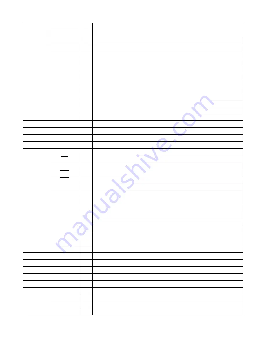
43
I-CDSW
I
CD mecha switch input.
44
I-SPEANA_L
I
A/D L-input for spectrum analyser level display.
45
I-SPEANA_R
I
A/D R-input for spectrum analyser level display.
46 ~ 48
I-KEY1 ~ I-KEY3
I
Key1 ~ Key3 input.
49
I-TU_SIG
I
Tuner signal input.
50
AVSS
–
GND.
51
O-PLL_CLK
O
PLL clock enable output.
52
O-PLL_CE
O
Chip enable output for tuner PLL.
53
O-CD_LED
O
CD flash window LED ON/OFF output.
54
O-KSCAN
O
Key scan output.
55
O-CD_CLK
O
CD clock output. (Not used)
56
O-CD_DATA
O
CD data output.
57
O-CD_CE
O
CD enable output. (Not used)
58
NC
–
Not connected.
59
I-JOG_B
I
Dial jog rotary encoder input B.
60
I-JOG_A
I
Dial jog rotary encoder input A.
61
I-VOL_B
I
Volume rotary encoder input B.
62
I-VOL_A
I
Volume rotary encoder input A.
63
I-REB
–
Deck 2 side-B recordable switch data input. "L" = REC. (Not used)
64
I-TM_BASE
I
Base input for clock.
65
I-CAM2
I
DECK2 CAM switch data input.
66
I-CAM1
I
DECK1 CAM switch data input.
67
P1/I-AUTO2
O/I
FL segment P1 output / DECK2 AUTO STOP switch data input.
68
P2/I-AUTO1
O/I
FL segment P2 output / DECK1 AUTO STOP switch data input.
69
P3/I-CST2
O/I
FL segment P3 output / DECK2 cassette detect switch data input.
70
P4/I-CST1
O/I
FL segment P4 output / DECK1 cassette detect switch data input.
71
P5/AM10K
O/I
FL segment P5 output / AM10K mode data input (not used).
72
P6/AMST
O/I
FL segment P6 output / AMST mode data input (not used).
73
P7/LW
O/I
FL segment P7 output / LW mode data input (not used).
74
P8/SW
O/I
FL segment P8 output / SW mode data input <HR only>.
75
P9/OIRT
O/I
FL segment P9 output / OIRT mode data input (not used).
76
P10/RDS
O/I
FL segment P10 output / RDS data input (not used).
77
P11/R+1
O/I
FL segment P11 output / REV data input.
78
P12/DEMO
O/I
FL segment P12 output / DEMO data input (not used).
79
VDD2
–
Power supply.
80
VLOAD
–
Power supply for FL display.
81
P13/C-JACK
O/I
FL segment P13 output / C-JACK data input.
82
P14/ECO-OFF
O/I
FL segment P14 output / ECO-OFF data input.
83
P15/P-LOGIC
O/I
FL segment P15 output / P-LOGIC data input (not used).
84 ~ 90
P16 ~ P22
O
FL segment P16 ~ P22 output.
91 ~100
G1 ~ G10
O
FL grid G1 ~ G10 output.
Pin No.
Pin Name
I/O
Description
Summary of Contents for NSX-VC38
Page 14: ... 14 SCHEMATIC DIAGRAM 1 MAIN 1 3 ...
Page 15: ... 15 SCHEMATIC DIAGRAM 2 MAIN 2 3 DECK SECTION HEAD 1 ...
Page 16: ... 16 SCHEMATIC DIAGRAM 3 MAIN 3 3 TUNER SECTION HR ...
Page 17: ... 17 SCHEMATIC DIAGRAM 4 MAIN 3 3 TUNER SECTION HS ...
Page 19: ... 19 SCHEMATIC DIAGRAM 5 FRONT DECK ...
Page 21: ... 21 SCHEMATIC DIAGRAM 6 AMP 1F ...
Page 22: ...WIRING 5 PT 22 1 2 3 4 5 6 7 8 9 10 11 12 13 14 15 A B C D E F G H I J K L M N O P Q R S T U ...
Page 23: ... 23 SCHEMATIC DIAGRAM 7 PT ...
Page 25: ... 25 IC BLOCK DIAGRAM ...
Page 26: ... 26 ...
Page 32: ... 32 CD TEST MODE ...