– 29 –
1
X-IN
I
A crystal oscillator (4.5MHz) is connected between these pins.
22
X-OUT
O
2
NC
–
Not connected.
3
CE
I
To enable the IC. Active "H".
4
DI
I
Digital data input from CPU (
µ
PD780226GF-017-3BA) when relevant key is operated.
Active "H".
5
CL
I
To clock in the data DI.
6
DO
O
Digital data output to CPU (
µ
PD780226GF-017-3BA).
7
TM-BASE
O
Outputs a reference clock signal (8Hz) for the clock.
8
MONO / BEAT
O
Outputs "H" when MONO / BEAT is switched.
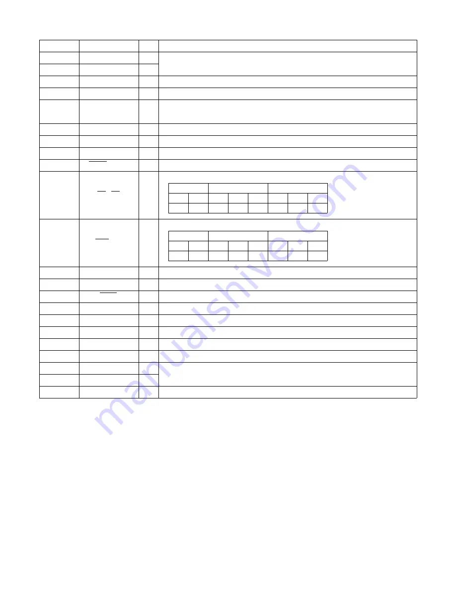
Output "L" or "H" as follows:
9
FM / SW
O
2 BAND
3 BAND
3 BAND
AM
FM
LW
MW
FM
MW
SW
FM
H
L
H
H
L
H
L
L
Outputs "L" or "H" as follows:
10
MW / SW
O
2 BAND
3 BAND
3 BAND
AM
FM
LW
MW
FM
MW
SW
FM
L
L
H
L
L
L
H
L
11
IF-MUTE
O
To control internal counter.
12
IF-IN
I
General purpose counter input.
13
TUNE
I
Receives "L" when station is tuned.
14
NC
–
Not connected.
15
AM-IN
I
Receives the AM local oscillator frequency signal.
16
FM-IN
I
Receives the FM local oscillator frequency signal.
17
VDD
–
Supply power to IC (+5V).
18
PD
O
PLL charge pump output.
19
A-IN
I
The MOS transistor used for PLL active low pass filter.
20
A-OUT
O
21
VSS
–
Ground.
Pin No.
Pin Name
I/O
Description
IC, LC72131D
Summary of Contents for NSX-VC38
Page 14: ... 14 SCHEMATIC DIAGRAM 1 MAIN 1 3 ...
Page 15: ... 15 SCHEMATIC DIAGRAM 2 MAIN 2 3 DECK SECTION HEAD 1 ...
Page 16: ... 16 SCHEMATIC DIAGRAM 3 MAIN 3 3 TUNER SECTION HR ...
Page 17: ... 17 SCHEMATIC DIAGRAM 4 MAIN 3 3 TUNER SECTION HS ...
Page 19: ... 19 SCHEMATIC DIAGRAM 5 FRONT DECK ...
Page 21: ... 21 SCHEMATIC DIAGRAM 6 AMP 1F ...
Page 22: ...WIRING 5 PT 22 1 2 3 4 5 6 7 8 9 10 11 12 13 14 15 A B C D E F G H I J K L M N O P Q R S T U ...
Page 23: ... 23 SCHEMATIC DIAGRAM 7 PT ...
Page 25: ... 25 IC BLOCK DIAGRAM ...
Page 26: ... 26 ...
Page 32: ... 32 CD TEST MODE ...