background image

-8-

Pin No.

Pin Name

I/O

Description

24 ~ 31

32

33

34

35

36

37

38

39

40

41

42

43

44

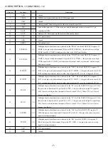
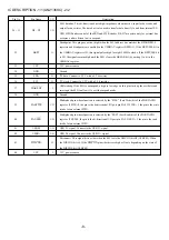
D0 ~ D7

BKPT

VCC

GND

SDA

SCL

_________

WAKEUP

GND

____

PA4/FWR

____

PA5/FRD

USBD-

USBD+

________

DISCON

VCC

8051 data bus. This bi-directiona bus is high-impedance when inactive, input for bus reads, and

output for bus writes. The data bus is also used to transfer data directly to and from internal EZ-

____

____

USB FIFOS under control of the FRD and FWR strobes. D0-D7 are active only for external bus

accesses, and are driven low in suspend.

Breakpoint. This pin goes active (high) when the 8051 address bus matches the BPADDRH/L

registers and breakpoints are enebled in the USBBAV register (BPEN=1). If the BPPULSE bit in

the USBBAV register is HI, this signal pulses high for eight 24 MHz clocks. If the BPPULSE bit

is LO, the signal remains high until the 8051 clears the BREAK bit (by writing 1 to it) in the

USBBAV register.

3.3V power source

Ground

I

2

C data. Connect to VCC with a 2.2 k resistor.

I

2

C clock. Connect to VCC with a 2.2 k resistor.

USBwakeup. If the 8051is unsuspend, a high to low edge on this pin starts up the oscillator and

interrupts the 8051to allow it  to exit the suspend mode.

Ground

Multiplexed pin whose function is selected by the “FWR” (Fast Write) bit of the PORTACFG

register. If FWR=0, the pin is the bi-directional I/O port pin PA4. If FWR = 1 the pin is the write

strobe for an external FIFO.

Multiplexed pin whose function is selected by the “FRD” (Fast Read) bit of the PORTACFG

register. If FRD=0, the pin is the bi-directional I/O port pin PA5. If FRD = 1 the pin is the read

strobe for an external FIFO.

USB D - signal. Connect to the USB D - signal.

USB D+ signal. Connect to the USB D + signal.

Disconnect. This signal drvives low when the 8051 sets the DISCON bit HI (USBCS3). When

________

the DISCON bit is LO, the DISCON pin either drivers high or floats, depending on the state of

the DISCOE bit (USBCS2).

3.3V power source

I/O

O

O

O

I

I/O

I/O

I/O

I/O

O

I

IC DESCRIPTION -1/1 (AN2136SC) -2/2

Summary of Contents for PV-HKU6401

Page 1: ...SERVICE MANUAL D A T A MODEM PV HKU6401 S M Code No 09 00B 350 8N2 YH3 S ...

Page 2: ... 2 SPECIFICATIONS Design and specifications are subject to change without notice ...

Page 3: ... 3 REF NO PART NO KANRI DESCRIPTION NO ACCESSORIES LIST 1 8A XMB 905 010 IB YH PV HKU6401 ...

Page 4: ...C IC USB6B1 87 A21 679 040 C IC BA033LBSG 87 A21 716 040 C IC M24C02WDW1T 87 A21 728 040 C IC SN74LVC07A 87 A21 773 040 C IC SN74LV165APW 87 A21 774 040 C IC SN74LV595APW 87 A21 775 040 C IC SN74LVC04APW 8A XMB 600 010 C IC AN2136SC MAIN C B D501 87 A40 841 040 C LED SML 310VT RED D502 87 A40 842 040 C LED SML 310MTGREEN X201 87 A70 271 080 C VIB XTAL 12 000MHZ FCX 03 CN401 8A XMB 601 010 CABLE AS...

Page 5: ... CONNECTOR 1 2 3 4 5 ESD PROTECTION IC202 M24C02WDW1T NON VOL IC301 BA033LBSG 3 3V REG C102 0 1 CPU 8 9 5 6 1 2 3 4 14 7 11 10 12 13 9 8 10 13 12 1 3 4 5 6 2 14 7 11 APW A A A A APW APW A A APW APW APW APW APW CONNECTOR FOR PCT TERMINAL ...

Page 6: ...14 44 1 3 5 7 3 1 5 7 12 14 10 8 12 14 10 8 12 1 2 3 5 4 1 1 3 4 8 7 5 3 4 5 1 3 5 7 8 3 1 1 3 5 7 14 12 10 8 5 7 8 9 11 13 1516 9 11 13 1516 BLU VLT RED YEL ORG BLK GRN CN104 CONNECTOR FOR PCT TERMINAL D502 USB READY D502 DATA 2 1 3 5 6 8 7 10 MAIN C B 1 2 3 4 5 6 7 8 9 10 11 12 13 14 15 A B C D E F G H I J K L M N O P Q R S T U ...

Page 7: ...e pin is the bi directional I O port bit PC2 If INT0 1 the pin is the active low 8051 INT0 interrupt input signal which is either edge triggered IT0 1 or level triggered IT0 0 Multiplexed pin whose function is selected by the INT1 bit of the PORTCCFG register If INT1 0 the pin is the bi directional I O port bit PC3 If INT1 1 the pin is the active low 8051 INT1 interrupt input signal which is eithe...

Page 8: ...SBBAV register 3 3V power source Ground I2 C data Connect to VCC with a 2 2 k resistor I2 C clock Connect to VCC with a 2 2 k resistor USBwakeup If the 8051is unsuspend a high to low edge on this pin starts up the oscillator and interrupts the 8051to allow it to exit the suspend mode Ground Multiplexed pin whose function is selected by the FWR Fast Write bit of the PORTACFG register If FWR 0 the p...

Page 9: ... 9 MECHANICAL MAIN PARTS LIST 1 1 REF NO PART NO KANRI DESCRIPTION NO 1 8A XMB 002 010 CABI TOP 2 8A XMB 003 010 WINDOW LED 3 8A XMB 001 010 CABI BOT 4 87 B10 024 310 VT2 1 7 6 W O ...

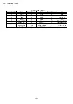
Page 10: ... Transparent Blue N Gold P Pink R Red S Silver ST Titan Silver T Brown V Violet W White WT Transparent White Y Yellow YT Transparent Yellow LM Metallic Blue LL Light Blue GT Transparent Green LD Dark Blue DT Transparent Orange GM Metallic Green YM Metallic Yellow DM Metallic Orange PT Transparent Pink LA Aqua Blue GL Light Green COLOR NAME TABLE ...

Page 11: ...2 11 IKENOHATA 1 CHOME TAITO KU TOKYO 110 8710 JAPAN TEL 03 3827 3111 920074 Printed in Singapore ...

Reviews: