background image

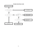
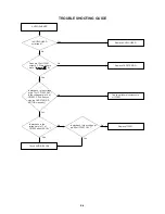
TROUBLESHOOTING GUIDE

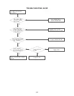
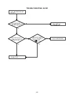
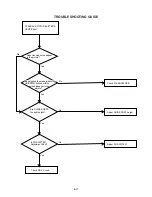
CYLINDER NOT ROTATING
DURING PLAYBACK AND
RECORDING

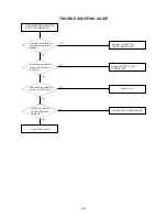
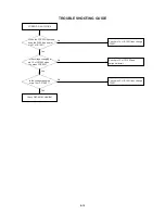
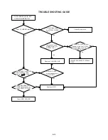
Check UNREG 12V line
of Main PCB.

Replace CYLINDER MOTOR.

Check R1059, R1080 and R1058.

Replace IC1001.

No

Yes

Yes

No

No

Yes

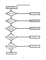
Is the voltage at pin 6 of
CP1002 about DC13V ?

In playback, is the
voltage at pin 3 of
CP1002 about DC1.2V ?

In playback, is the
voltage at pin 44 of
IC1001 DC5V Pulse and
is the voltage at pin 46 of
IC1001 about DC1.5V ?

E-8

Summary of Contents for VX-G142

Page 1: ...ec NTSC Playback SP only 33 35mm sec PAL SP 4 hours 20 minutes with E 260 tape LP 8 hours 40 minutes with E 260 tape NTSC Playback SP only 3 hours with T 180 tape 1 0Vp p 75 ohm unbalanced 1 0Vp p 75...

Page 2: ...F SCHEMATIC DIAGRAM PRINTED CIRCUIT BOARDS SYSCON Y C SCHEMATIC DIAGRAM SYSTEM CONTROL SCHEMATIC DIAGRAM TUNER AUDIO SCHEMATIC DIAGRAM POWER IN OUT SCHEMATIC DIAGRAM MICON SCHEMATIC DIAGRAM CHROMA SCH...

Page 3: ...a tube or tape for safety or which are assembled in the condition that these do not contact with the printed board The inside wiring is designed not to get closer to the pyrogenic parts and high volt...

Page 4: ...rve the chroma signal There are two types of the new alignment tape CH 1B for NTSC and CH 2 for PAL On each tape four signals 1 4 are recorded for the times and in the order shown below The TTV MP1 fo...

Page 5: ...1 3 Front Cabinet Back Cabinet 1 2 2 1 1 1 Fig 1 1 CAUTION BEFORE REMOVING THE ANODE CAP DISCHARGE ELECTRICITY BECAUSE IT CONTAINS HIGH VOLTAGE BEFORE ATTEMPTING TO REMOVE OR REPAIR ANY PCB UNPLUG THE...

Page 6: ...ection in the direction of arrow B Remove the 2 screws 6 Unlock the 2 supports 7 and remove the Jack Plate in the direction of arrow C Remove the screw 8 Unlock the support 9 and remove the Syscon PCB...

Page 7: ...Spring Fig 2 4 1 1 2 1 Unlock the 2 supports 1 2 Remove the Cassette Side R 3 Remove the Pack Spring 4 Remove the Locker Spring 5 Unlock support 2 6 Remove the Locker R Cassette Side L Cassette Side R...

Page 8: ...n Arm Ass y 5 Remove the Tension Band Ass y 6 Remove the Tension Lever 2 Ass y Fig 2 7 Tension Arm Spring 2 NOTES 1 2 Install the Tension Band Ass y without twisting it Oil the area marked with A in F...

Page 9: ...lyslider Washer NOTES 1 2 Do not touch the head by any means when replacing the Audio Control Head Use gloves After replacement confirm the following adjustments a MECHANICAL ADJUSTMENTS ITEM 2 2 b ME...

Page 10: ...e the Center Pulley 3 Remove the Polyslider Washer 2 4 Remove the Center Pulley Spring 5 Remove the Idler Arm Ass y 6 Remove the 2 Polyslider Washers 3 7 Remove the Clutch Gear T Ass y and Clutch Gear...

Page 11: ...lder Loading Lever Fig 2 14 Loading Gear T Marker Disconnect the following connector CP4105 on the Head Amp PCB Remove the 3 screws 1 Remove the Capstan DD Unit NOTE Use the specified screw to hold th...

Page 12: ...p up the sides of the Rubber Cap in the direction of the arrow and remove one side of the support Refer to Fig 3 2 2 GND on the CRT Screwdriver Alligator Clip Support CRT GND on the CRT Rubber Cap CRT...

Page 13: ...linder Cylinder Motor Cylinder Sensor Data Syscon to Servo Decibel Direct Current Direct Drive Motor Unit Demodulator Detector Deviation Emitter Emitter Follower Emphasis Encoder Envelope End of Tape...

Page 14: ...or Separation Transistor Tracking Trick Playback Test Point Unregulated Volt Voltage Controlled Oscillator Video Intermediate Frequency Vertical Pulse Voltage Display Video Playback Variable Resistor...

Page 15: ...r Refer to the figure below 2 TAPE RUNNING SYSTEM When cleaning the tape transport system use the gauze moistened with isopropyl alcohol 3 CYLINDER Wrap a piece of chamois around your finger Dip it in...

Page 16: ...e by setting VOLUME to minimum While holding down VOLUME button on front cabinet press key 6 on remote control simultaneously ADDRESS and DATA should appear as FIG 1 Fig 1 ADDRESS is now selected and...

Page 17: ...P0 Post P1 Post FE Head Cylinder Unit Auto Head Cleaning Head Amp PCB Audio Control Head 12 13 14 15 16 17 18 19 20 21 Loading Motor Pinch Roller Block Cam Gear Cassette Opener Brake Bracket Reel T L...

Page 18: ...29 30 31 32 33 Capstan Brake Ass y Bottom Plate Clutch Gear S Ass y Idler Arm Ass y Center Pulley Clutch Gear T Ass y FRONT LOADING UNIT 9 1 2 3 4 5 6 7 8 Side Bracket L Top Bracket Ass y Side Bracke...

Page 19: ...2 JG024 JG100A Remarks Stair Steps 6KHz Color Bar 1KHz Playback Take Up Torque Fast Forward Torque Rewind Torque Brake Torque Take up Reel Supply Reel Guide Roller Adjustment X Value Adjustment Reel D...

Page 20: ...nd JG162H Connect the Syscon PCB to the CRT PCB with the cable JG162Y Short circuit between TP1001 and Ground with the cable JG154 Refer to MAJOR COMPONENTS LOCATION GUIDE The EOT BOT and Reel Sensor...

Page 21: ...hich weighs between 350g and 500g on the Cassette Tape to keep it steady when you want to make the tape run without the Front Loading Unit 9 Do not place an object which weighs over 500g When you acti...

Page 22: ...olerance replace the appropriate parts as follows 2 TAPE RUNNING CONFIRMATION AND ADJUSTMENT Tape running is adjusted precisely at the factory Normally it is not necessary to make adjustments It is ne...

Page 23: ...the screw 3 Refer to Fig 2 2 until the height of the A C head reaches the position against the tape as shown in Fig 2 3 When the control head height is not correct When you must turn the screw more t...

Page 24: ...MAJOR COMPONENTS LOCATION GUIDE VCR SECTION SYSCON TU6001 CP6115 IC4001 IC103 CP1002 IC601 TP4501 IF IC6001 CP6001 L6012 VR6001 L6011 CP4001 TP4001 TP4002 TP1001 D2 1...

Page 25: ...ing press both VOL DOWN key on the set and the channel button 4 on the remote control simultaneously and adjust the Tracking button until the arising to the down of the Head Switching Pulse becomes 6...

Page 26: ...NTS 39 5MHz Fig 3 3 3 4 COLOR LEVEL CONDITIONS MODE STOP INSTRUCTIONS 1 2 Connect the oscilloscope to TP4501 When the Y LEVEL is 100 adjust the VR6001 until the MAGENTA Section LEVEL becomes 45 5 Refe...

Page 27: ...MAJOR COMPONENTS LOCATION GUIDE TV SECTION MAIN SCREEN VOLUME FOCUS VOLUME FB401 T501 CRT J801 TP801 TP803 VR502 TP401 D3 1...

Page 28: ...ODE2 1 2 RED BIAS 3 GREEN BIAS 4 BLUE BIAS 5 GREEN DRIVE 6 BLUE DRIVE 7 NEXT 8 END Fig 4 2 ADJUSTMENT MODE3 1 BRIGHT 2 CONTRAST 3 COLOR 4 TINT 5 SHARPNESS 6 E RGB CONT 7 NEXT 8 END The adjustment item...

Page 29: ...te control until the SHIFT quantity of the OVER SCAN on upside and downside becomes minimum 4 10 OSD HORIZONTAL 1 2 3 Using the remote control set the brightness and contrast to normal position Activa...

Page 30: ...e display of Fig 4 3 and press the channel button 3 on the remote control Adjust the VOLTS RANGE VARIABLE knob of the oscilloscope until the range between white 100 and 0 is set to 4 scales on the scr...

Page 31: ...rom the green raster pattern to the crosshatch pattern Combine red and blue of the 3 color crosshatch pattern on the center of the screen by adjusting the pair of 4 pole magnets Combine red blue magen...

Page 32: ...IC502 DC7 7V Does RY501 work Check P CON 5V line Check IC502 D511 and D512 Check IC502 Check pins 62 and 63 of IC101 and peripheral circuit Check IC506 Q507 and the peripheral circuit Check Q504 RY50...

Page 33: ...RN ON 2 Is CP810 inserted Is the voltage at C507 about 160V Insert CD810 Check the circuit between F501 C507 and R501 Check IC501 and the peripheral circuit Yes Yes Yes Yes No No No No Replace F501 Re...

Page 34: ...peripheral circuit Check Q353 and peripheral circuit Is the voltage at pin 29 of IC601 changed from DC10 8V to DC9 9V when pressing VOLUME UP or DOWN key Yes Yes Is the voltage at pin 1 corrector of...

Page 35: ...V line Adjust Brightness and Contrast Is the voltage at pin 17 of IC601 DC9V Is the voltage at pin 41 of IC601 DC5V Is the voltage at pin 8 38 of IC601 DC5V Is the signal at pin 12 13 and 14 of IC601...

Page 36: ...put Is the waveform 12 13 and 14 of IC601 normal Is the waveform at pin 42 of IC601 normal Is the waveform at pin 40 of IC601 normal Is the color signal received Is the color set to minimum NO COLOR R...

Page 37: ...it of IC601 Check peripheral circuit of IC101 Check R452 and FB401 Is the normal signal at pin 4 of IC 401 input Is the normal signal at pin 38 of IC101 output Is the voltage at pin 6 of IC402 DC25V C...

Page 38: ...heck TAPE LOADIG LOADING BELT MODE SWITCH DD MOTOR and CYLINDER MOTOR Does it Power off in about 3 seconds Yes No Check REEL SENSOR and REEL BELT Does it Power off in about 6 seconds Yes No Check REEL...

Page 39: ...Replace CYLINDER MOTOR Check R1059 R1080 and R1058 Replace IC1001 No Yes Yes No No Yes Is the voltage at pin 6 of CP1002 about DC13V In playback is the voltage at pin 3 of CP1002 about DC1 2V In play...

Page 40: ...o Yes Is AUDIO HEAD scratched Does pin 15 of IC1001 output a 3 0Vp p square wave 3 0V Check AUDIO BLOCK In playback is the voltage at pin 17 of CP1002 about DC1 6V In playback is the voltage at pin 14...

Page 41: ...MOTOR When a cassette is inserted is the voltage at pin 49 of IC1001 5V When a cassette is inserted is the voltage between pins 1 and 2 of CP1002 When cassette is not inserted is EOT BOT PULSE at EMMI...

Page 42: ...FRONT LOADING GEARS Defective CASSETTE or FRONT LOADING UNIT In another cassette tape does the same problem appear In covering the infrared sensor is pin 2 and 3 of IC1001 5V When inserting cassette i...

Page 43: ...of CP1002 and peripheal circuit Check pin 45 of IC1001 lines change IC1001 Check DECK MECHANISM Is the voltage changing at pin 14 of CP1002 Is the voltage changing at pin 12 of CP1002 when you press...

Page 44: ...k R1059 R1080 R1058 and D1003 No Yes Does PG PULSE signal appear at pin 13 of IC1001 No No No Yes Is the voltage at pin 6 of CP1002 UNREG 12V Does DC5V PULSE signal appear at pin 44 of IC1001 Is the v...

Page 45: ...age at pin 3 of CP1002 1 2V In playback is the voltage at pin 3 of CP1002 about 1 2V When sloeing CYLINDER is the voltage 3 8V No Yes Replace CYLINDER MOTOR Replace IC1001 No No Yes Yes 5V Is FG Pulse...

Page 46: ...k IC4101 and CYLINDER UNIT Check CONTROL HEAD No Yes By manual tracking does the DC level at pin 6 of CP4001 change In auto tracking is the voltage at pin 5 of IC1001 more than DC1 85V No No Does the...

Page 47: ...ROTATING No Yes Replace CAPSTAN BELT No Check REEL SENSOR and that the voltage at pin 10 of CX1003 is DC5V No Does CAPSTAN DD MOTOR rotate Is CAPSTAN BELT OK Yes Does REEL SENSOR PULSE signal appear...

Page 48: ...No Adjust GUIDE POST height Adjust PG SHIFTER No Does tracking noise appear in the picture Yes Yes Are GUIDE POSTS the right height No Check PB Y circuit Is PG SHIFTER Adjustment 6 5H Yes By adjustin...

Page 49: ...es Is the voltage at pins 12 28 and 54 of IC4001 5V No Yes Check IC4002 and the peripheral cicuit No Replace IC4001 Replace IC4001 No No Yes Is there Y signal at pin 27 of IC4001 and there CHROMA sign...

Page 50: ...7 and the peripheral circuit Replace IC4002 Does FM ENVELOPE appear at TP4002 Does CHROMA signal appear at pin 27 of IC4001 Does COMPOSITE signal appear at pin 16 of IC4002 Does COLOR BURST signal app...

Page 51: ...p p Is there FM signal at pin 11 of IC4001 140mVp p No Yes Replace IC4001 No Replace IC4002 No Yes Is VIDEO waveform at pin 6 of IC4001 over 500mVp p and are there any noise Yes Yes Check J4501 Is VID...

Page 52: ...in 29 of IC4001 No No No No Replace IC4101 Check IC4101 and peripheral circuit Replace J4501 Check VIDEO input circuit Does VCR signal appear at pin 53 of IC4002 Does FM signal appear at pin 8 of CP40...

Page 53: ...igh No No Does AUDIO signal appear at pin 7 of IC5001 Check AUDIO HEAD for debris of stains Check that the connector from AUDIO HEAD is fully inserted to CP4106 Replace IC 5001 If the pin 52 of IC1001...

Page 54: ...15 of CP1002 5V In playback is the voltage at pin 14 of CP1002 2 5V Replace IC1001 Does DD MOTOR rotate now If not replace DD MOTOR Check pins between 45 and 47 of IC1001 and peripheral circuit Replac...

Page 55: ...cuit Is there AUDIO signal at pin 14 of IC5001 Check the lead wire and connector to A C HEAD Check the circuit between audio out of Tuner and pin 10 of IC5001 No No Yes Yes No No No Yes Yes Yes Is the...

Page 56: ...ETTE IN AND DOWN UNIT HAS NO FUNCTIONS No Yes Yes No Check Operation PCB Does VCR operate with the remote control Check IC1001 Check LOADING MOTOR MODE SWITCH and the peripheral parts Does mode indica...

Page 57: ...CYLINDER UNIT and IC4101 circuit No No Check the circuit from VIDEO input jack to IC4001 from Tuner Pack to IC4001 Check the peripheral circuit of Q4007 Q4009 Replace IC4001 Replace IC4101 RECORDING...

Page 58: ...uit Replace IC6001 and check peripheral circuits Check 9V and 5V line Check Q6002 Is there VIDEO signal at pin 20 of IC6001 Is defect present when replacing the IF PCB Is the voltage at pin 6 of TU600...

Page 59: ...YS IN I COLOR SYSTEM input from Y C SECAM CHROMA IC 24 DV SYNC O DV SYNC output for Y C IC 25 AFT I AFT S CURVE input 26 KEY A I KEY A input 27 KEY B I KEY B input 28 VL O Band output 29 VH O Band out...

Page 60: ...ut 54 VCR MUTE O VCR mute output 55 SST I Serial data input 56 STS O Serial data output 57 SCLK O Serial clock output 58 STRB O Strob output 59 SIF O SIF selection 60 AUDIO A O Switching output of HI...

Page 61: ...HI FI L I Input selection of audio type 28 AUTO DET IN I Ground 29 BILINGUAL L I Input selection of audio type 30 STEREO L I Input selection of audio type 31 2HEAD 4HEAD I Input terminal for heads se...

Page 62: ...ights at REC mode 61 T REC LED O Lights at T REC mode 62 CLOCK 0 Terminal to connect the oscillator 63 CLOCK 1 Terminal to connect the oscillator 64 VSS Ground 65 ATR LED O Lights at ATR mode 66 PLAY...

Page 63: ...o Signal Input Terminal 29 AUDIO OUT O Output the Audio Signal through the Attenuator 30 APC FILTER Connects the APC filter for the Chromatic Demodulation 31 Y2 IN I Input the Y signal that is separat...

Page 64: ...OEC9032B SERVO TIMING CHART DRUM PG 3 PIN DRUM FG 1 PIN VIDEO H SW 8 PIN V SYNC 2 PIN PB CTL 9 PIN CTL OUT 0 PIN 6 5 H 6 5 H REC PB 30 Hz 720 Hz 30 Hz 30 Hz WAVEFORM CHANGES DEPENDED ON THE TAPE SPEE...

Page 65: ...STOP 2 FF REW SW 3 SW 2 SW 1 SW 0 DECK MODE VOLTAGE V 0 5 5 5 5 5 5 5 5 5 5 0 0 5 5 0 5 5 0 0 5 5 0 5 0 0 5 5 5 5 5 5 5 5 0 0 5 5 5 0 0 0 0 0 5 5 0 5 0 0 0 0 EJECT COMPLETE CASS IN COMPLETE UL START...

Page 66: ...4605 3 TRANSISTOR 3PIN 3PIN 2PIN 10PIN 4PIN 2SC4160 ORI 2SD2396 J K PST600H NJM7805FD UPC574J T OEC9029A TLP621 GR NJM7809FA DTC114ESTP DTA114TSTP 2SD2089 2SK2397 01MR 2SA1015Y TPE2 DTC114TKT147 2SA10...

Page 67: ...2MHZ Q405 H DRIVE Q406 H OUTPUT IC401 TA8403K 2 4 V OUTPUT DY F S 9 HV FB401 7 9 F 8 J801 3 DEGAUSS COIL AC IN G AMP Q805 B AMP Q806 R AMP Q804 CONSTANT VOLTAGE VR502 SW Q356 BUFFER Q612 SW Q408 SW Q4...

Page 68: ...AMP Q4016 BUFFER Q4101 BUFFER Q4006 BUFFER Q4005 ENV DET 46 BUFFER Q4010 37 BUFFER Q4017 VCR VIDEO OUT AE FE HEAD CH2 L F CH1 2 S CH1 R F 2 3 4 CP4101 TUNER AUDIO IF CYL CYL PG CYL FG CYL DRIVE 1 3 5...

Page 69: ...SENS Q1054 63 62 CLOCK 0 CLOCK 1 X1001 8MHz Q756 POWER LED SW P CON 5V Q757 POWER SW D793 D791 D792 D794 44 PWM 0 12 DFG IN 13 DPG IN 15 CFG OUT KEY B KEY A CH UP PLAY VOL DOWN TV STOP EJECT POWER ON...

Page 70: ...6 5 12 LIM FM DET 10 VIF SIF IC6001 M52313SP 11 2 TU6001 5 4 1 CF6004 SAW FILTER Q6003 AMP 2 VCR AUDIO OUT Q6101 T AUDIO MUTE TU MUTE Q6104 BUFFER AFT S CURVE TV 5 4 6 2 1 3 T5001 Q5004 BIAS OSC AUDI...

Page 71: ...758 CY759 PRINTED CIRCUIT BOARDS OPERATION 1 IC4101_2 C4112 C4113 C4114 C4115 C4119 C4120 R4111 C4110 C4127 C4108 C4104 R4109 C4102 C4105 C4106 R4102 C4103 R4103 R4113 Q4101 R4104 W801 HEAD AMP IF C60...

Page 72: ...W05 W08 W14 W13 L6012 IC6001 L6009 CF6001 VR6001 L6010 L6007 JP6001 C6002 L6002 L6011 CF6003 C6021 JP6003 JP6004 R6006 L6005 R6007 Q6003 L6004 CP6001 R6005 CF6005 C6019 3 CF6004 C6005 1 R6020 JP6009 J...

Page 73: ...R4113 Q4101 R4104 W801 HEAD AMP IF C6014 R6009 R6010 R6008 C6007 C6009 C6027 C6020 R6013 C6022 C6023 1 R6014 R6015 R6018 C6008 C6017 Q6002 R6016 R6001 R6003 C6006 C6001 JP6006 C6010 JP6009 JP6007 C603...

Page 74: ...C114TS POWER SW Q756 DTC114TS POWER LED SW Q758 DTC114TS PLAY BACK LED SW D792 EQ 552F9T POWER C751 100P B C781 0 001 B C779 0 001 B SW751 SKHVBED010 POWER ON OFF SW799 SKHVBED010 CH DOWN SW795 SKHVBE...

Page 75: ...TICE NOTE THIS SCHEMATIC DIAGRAM IS THE LATEST AT THE TIME DURING PLAYBACK MEASURED WITH THE DIGITAL TESTER NOTE THE DC VOLTAGE AT EACH PART WAS CYL_PG A CYL B A CYL_FG A GND_B CYL_DRIVE_A CYL_DRIVE_A...

Page 76: ...0 4 7K R6011 56 R6004 1 1 5K R6018 2 2K R6015 430 L6009 10uH L6005 1 2uH L6004 12uH L6010 33uH L6007 6 8uH VR6001 22K Q6002 2SA1037K BUFFER CP6001 6035B 12Z002 T 1 10 11 12 2 3 4 5 6 7 8 9 L6002 100uH...

Page 77: ...09 R1004 W197 W196 R5002 R5001 R5007 R5005 C5005 R5010 C5008_1 R5004 R1015 C5029 W805 C5028 R5027 Q4015 Q4007 Q4005 Q4006 Q4004 Q4012 Q4009 Q4016 Q4001 Q4010 Q4011 Q4013 Q4017 Q1018 Q1017 C4076 R4036...

Page 78: ...362 W184 W293 W213 W319 W320 W214 W222 W217 W218 W216 W221 W224 R1009 W201 W188 W242 W284 W151 W152 D1010 W089 W085 W084 W093 W092 W098 W101 W414 W113 W121 W055 W065 W170 W333 C4037 W061 W377 W378 W37...

Page 79: ...9 R4021 C4019 R4037 R4039 W810 W846 R670 W887 W894 W891 W909 R671 R6103 W970 W969 W857 W832 W831 W911 L6102 W844 B6101 W813 W886 W890 W913 W843 W842 W943 W910 W908 W838 W917 W897 W902 W927 W907 W880 W...

Page 80: ...4054 680 R4002 820 R4012 1K R4007 1K R4055 12K R4029 680 R4034 1 2K R4048 820 R4049 2 2K R4047 82K R4045 120K R4033 1M R4028 1 5K R4064 330 R4065 10K R4046 68 R4025 1K R4026 1M R4030 4 7K R4041 47K R4...

Page 81: ...10K R1029 10K R1052 10K D1003 1SS133 D1008 1SS133 D1005 11ES1 D1010 11E1N D1013 11E1 D1009 1SS133 TP1001 SERVICE DESCRIBED IN PARTS LIST ONLY CRITICAL FOR SAFETY USE ONES ARE SINCE THESE PARTS MARKED...

Page 82: ...0 47 50V KA L5005 1mH L5001 100uH 0607 L6105 100uH L6102 0 47uH W813 W912 W924 W923 W844 W911 W971 W886 W919 W814 W805 W873 W963 W982 W930 R5018_1 68 R6116 100K R6115 390K R6306 150K R6309 390K R6308...

Page 83: ...18 68 R4505 100 R4519 270 1 2W R1099 10K R4502 220 R1097 220 1 4W R1096 10K R1098 10K R4514 100K R4504 75 R1089 1K R1100 1K R1101 10K R4512 220 TP4501 V OUT DESCRIBED IN PARTS LIST ONLY CRITICAL FOR S...

Page 84: ...R6503 4 7K R185 150 1 4W R186 220 1 4W R168 1K R165 1K R162 1K R121 4 7K R136 1K R140 5 6K R172 4 7K R110 22K R163 2 2K R189 10K R184 15K R141 10K R187 18K R134 10K R132 1 5K R159 10K R155 270 R156 2...

Page 85: ...3 10M R664 10M R665 10M R666 8 2M R610 390 R631 270 R669 1 5K R635 1 8K R641 27K R616 470 R619 10K R657 4 7K R670 1K R656 100 D606 1SS133 D608 LFB 01L D609 LFB 01L D610 LFB 01L D611 LFB 01L DESCRIBED...

Page 86: ...16V YK C355 47 16V KA Q351 2SC2120Y SOUND OUTPUT Q354 2SC2412K SWITCHING Q353 2SC1815Y SOUND OUTPUT Q352 2SA950Y SOUND OUTPUT Q356 DTC114TKA SWITCHING W947 W855 R360 1 1 2W R359 1 1 2W R358 180 R362 1...

Page 87: ...NOTE THIS SCHEMATIC DIAGRAM IS THE LATEST AT THE TIME W936 W928 W938 W929 D705 1SS133 D703 1SS133 D706 11E1 T REC_LED REC_LED V REC_ST H AT 5 6V GND REMOTE KEY A KEY B PB_LED TV_POWER H J 17 OPERATION...

Page 88: ...6 W035 D516 IC506 C530 C533 C529 R806 R809 C802_1 D801 D802 Q801 R804 W017 R423 D402 W824 W030 W007 R422 C524 D519_1 C523 W043 FH503 FH504 C518 Q507 D528 R532 R533 R555 R554 R553 D529 D535 D518 VR502...

Page 89: ...X19 C485_1 1 50V YK C421 1000 35V VZ C418_1 1 160V DURING PLAYBACK MEASURED WITH THE DIGITAL TESTER NOTE THE DC VOLTAGE AT EACH PART WAS OF PRINTING AND SUBJECT TO CHANGE WITHOUT NOTICE NOTE THIS SCHE...

Page 90: ...33K 1 2W R554 27K 1 2W R558 12K R502 220 1 4W R507 5 6K R565 180K 1 2W R506 560K 1 2W R566 150K 1 2W R511 22K R523 10K R522 47K R525 22K R527_1 20K R524 10K 1 4W D506 1R5NU41 D518 1SS133 D512 21DQ09N...

Page 91: ...30 R816_1 330 R804 390 R809 1K D801 1SS133 D802 1SS133 Q806_1 2SC3468 BLUE AMP Q805_1 2SC3468 GREEN AMP Q804_1 2SC3468 RED AMP W888 W855 W842 W863 W862 W805 W813 W836 TP801 TP802 TP803 R810_1 12K 2W R...

Page 92: ...TE THIS SCHEMATIC DIAGRAM IS THE LATEST AT THE TIME B351 BL01RN1 A63T6 R360 82 1 2W C353 0 001 B C354 0 0022X CD353 CP353 CH23043A 1 2 3 J353 HSJ0846 01 200 EAR JACK 1 2 3 W841 L353 HF57T18 5 10 10 SO...

Page 93: ...FE HEAD GND REC Y C PB Y C P CON 5V P CON 9V CP6001 VE4666 PCB350 TV AUDIO TV VIDEO 2 AGC CTL AGC IF 12 11 10 9 8 7 6 5 4 3 1 AFT S CURVE GND PCB330 CP4101 CP4102 H5001 FPC CH1 R F CH1 2S CH1 CH2 UN4...

Page 94: ...iv 9 REC PB 200mV 10V div 10 12 REC PB 0 5V 0 2V div REC PB 20mV 0 5V div 11 Y C WAVEFORMS REC PB 0 5V 5V div 13 REC PB 20mV 5V div 14 REC PB 2V 5V div 14 REC PB 0 5V 5V div 15 REC PB 1V 2U div 16 REC...

Page 95: ...N HEAD AMP 2V 5V div 34 5V 20U div 35 REC 50mV 10U div 42 50V 20U div 36 CRT REC PB 10mV 1s div 43 50V 20U div 37 PB 50mV 50V div 44 The following waveforms were measured at the point of the correspon...

Page 96: ...5 136 215 215 215 205 153 146 126 127 127 128 129 149 150 131 132 133 134 135 205 206 A SP352 207 214 PCB390 EARPHONE PCB 101 130 130 112 213 205 PCB340 POWER SW PCB 213 140 205 151 151 151 152 117 11...

Page 97: ...125 PCB330 HEAD AMP PCB 103 107 110 106 111 PCB010 SYSCON PCB 205 208 208 209 209 209 210 216 216 221 218 218 219 220 PCB030 OPERATION 1 PCB 137 211 211 211 211 109 201 PCB350 IF PCB A 108 105 105 120...

Page 98: ...410 SCREW TT B BRAZIER 3 8 11 121 IF SHIELD BOTTOM 1 205 S1 106 30A 240 SCREW TAP P 3 12 3 122 METAL SPACER 3 206 S1 106 308 040 TAP P 3 8 8 123 SPACER FBT 1 207 S1 106 306 040 UIT 3 6 3 124 SHIELD C...

Page 99: ...3 310 512 311 312 321 316 309 304 305 316 313 319 320 503 306 308 322 M101 503 323 504 511 324 325 329 515 327 307 326 334 338 337 335 340 336 516 339 516 509 333 332 331 330 UN4001 M2003 H5001 315 51...

Page 100: ...D VIEW BOTTOM VIEW 342 M2001 344 346 352 351 348 349 350 347 345 366 364 365 507 515 359 517 361 362 367 368 355 356 353 354 357 357 506 504 503 358 343 369 SW101 502 502 504 507 341 363 504 504 370 3...

Page 101: ...FRONT LOADING UNIT 9 EXPLODED VIEW 421 403 420 404 407 405 401 410 408 421 416 417 406 409 419 425 402 415 412 411 411 424 422 413 414 422 423 418 M1 3...

Page 102: ...00 5N0 POLY W CUT 1 6 6 0 5 2 333 S5 OP2 002 170 REEL T 1 508 S2 Q31 54B 3N0 PW 3 1 5 4 T0 13 1 334 S5 OP4 004 460 CATCHER P5 VP 1 509 S1 0A1 306 040 SCREW WASHER A M3 6 2 335 S5 OP6 004 650 SUB BRAKE...

Page 103: ...CAP E 100 6 3V D705 87 020 465 010 DIODE 1SS133T C1011 87 010 112 080 CAP E 100 16V D706 S2 8T1 1E1 N10 DIODE 11E1N TA1B2 C1013 87 010 221 080 CAP E 470 10V D1001 S0 013 000 300 PHOTO DIODE SLR 938C C...

Page 104: ...Q4010 89 110 372 080 TR 2SA1037AKT X1001 S0 0CA 8R0 050 X TAL 8 0MHZ Q4011 89 110 372 080 TR 2SA1037AKT X4001 S0 0CA 4R4 040 X TAL 4 4336MHZ Q4012 89 110 372 080 TR 2SA1037AKT Q4013 89 324 122 080 TR...

Page 105: ...00V D528 87 017 712 080 ZENER UZ 5 6BCB TA C418 S0 E7T B01 0M0 CAP E 1 160V D529 87 020 465 010 DIODE 1SS133T C421 87 010 397 010 CAP E 1000 35V D531 87 020 465 010 DIODE 1SS133T C422 87 016 322 010 C...

Page 106: ...3V VARIABLE RESISTOR IC VR502 S1 263 Q2B TC0 VOL RH063MCS2R07A IC4101 S0 3FG 741 1M0 IC LA7411M CONNECTORS TRANSISTOR CD005 S6 870 141 0A0 CORD CONN 8701410A CD810 S6 812 809 2A0 CORD CONN 8128092A Q...

Page 107: ...030 CER FIL TPS6 0M CF6003 S0 12T 6R0 020 CER FIL SFE6 0M CF6004 S0 2E2 39R 5A0 FILTER SAW J1953M CF6005 S0 12T 6R0 050 CER FIL CDSH6 0ME44K CF6008 S0 12T 041 010 FILTER CERA MKT41 5MA110P EARPHONE P...

Page 108: ...920074 Printed in Japan 2 11 IKENOHATA 1 CHOME TAITO KU TOKYO 110 8710 JAPAN TEL 03 3827 3111...

Reviews: