-19-
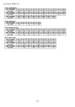
1-4
5
6
7
8
9
10
11
12
13
14
15
16
17
18
19
20
21
22
23
24
25
26
27
28
29
30
31
32
33
34
35
36
37
38
39
40
41
42
43
44
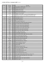
Pin No.
Pin Name
I/O
Description
IC DESCRIPTION-2/2 (MN101C439-AE)-1/2
COM3-0
VLC3
VLC2
VLC1
VDD
OSC2
OSC1
VSS
XI
XO
MMOD
VREF-
K-FUNC
K-P/S
ACIN
VDIN
K-RMC
SWDO
SWEASS
SWR/H
VREF+
SWIL
PC
CD-RW
______________
CD-RW
SUBQ
SQCK
BEEP
RST
NRST
STAT
MLD
MDATA
MCLK
BLKCK
RSENSOR
AHC-4/5
—
_____________
PU-ON
________________
EASSON
DSL2
O
—
—
—
—
O
I
—
I
O
I
—
I
I
I
I
I
I
I
I
—
I
O
O
O
I
O
O
—
O
I
O
O
O
I
I
I
—
O
O
O
LCD common.
—
—
—
LCD power supply.
Microprocessor main clock oscillator output. (Not connected)
Microprocessor main clock oscillator input.
Ground.
Sub-clock oscillator input.
Sub-clock oscillator output. (Not connected)
Processor mode is not used. Connected to VSS.
VSS.
Function key input.
PLAY, STOP KEY input.
AC adapter detection.
Battery voltage detection.
Wired remote control input.
Digital out ON/OFF input. L= ON.
Select input of EASS mode. Refer to A/D value table.
Resume/hold switch input.
VCC.
Limit switch input.
Power off output of CD servo driver. L= Power off.
CD-RW playback gain-up select output. H= Gain-up.
CD-RW playback gain-up select output. L= Gain-up.
H/A power-down output.
Gain-up select output by EASS. During EASS ON= L.
Buzzer output of headphones.
Microprocessor reset input.
DSP reset output.
STAT input of DSP.
MLD output of DSP.
MDATA output of DSP.
MCLK output of DSP.
BLKCK input of DSP.
Wireless remote control sensor signal input.
Select input of AHC-4 or AHC-5. AHC-4=H. AHC-5=L.
Not used.
Power down output of H/A.
Select output of gain-up by EASS. During EASS ON= L.
DSL2 control output of headphones. DSL2= H. DSL1/OFF= L.
Summary of Contents for XP-V420
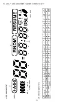
Page 8: ...8 FL AHC 7 GRID ASSIGNMENT ANODE CONNECTION 1 1 GRID ASSIGNMENT ANODE CONNECTION...
Page 9: ...9 SCHEMATIC DIAGRAM 1 1...
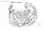
Page 10: ...10 WIRING 1 2 MAIN COMPONENT SIDE...
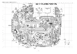
Page 11: ...11 WIRING 2 2 MAIN CONDUCTOR SIDE...
Page 26: ...26 CD MECHANISM EXPLODED VIEW 1 1 DA23LH 6 A C B 3 1 7 4 5 2 8...


