– 4 –
NOTE ON BEFORE STARTING REPAIR
Charging voltage (V)
Discharging
Rated power (W)
Parts number
(C101, 102)
resistor (
Ω
)
25-48
100
3
87-A00-247-090
49-140
220
5
87-A00-232-090
Note:
The reference numbers (C101, C102) of the electrolytic capacitors can change depending on the models. Be sure to check the
reference numbers of the charging capacitors on schematic diagram before starting the discharging work.
2. Check items before exchanging the MICROCOMPUTER
Be sure to check the following items before exchanging the MICROCOMPUTER. Exchange the MICROCOMPUTER after confirming
that the MICROCOMPUTER is surely defective.
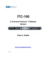
2-1. Regarding the HOLD terminal of the MICROCOMPUTER
When the HOLD terminal (INPUT) of the MICROCOMPUTER is “H”, the MICROCOMPUTER is judged to be operating correctly.
When this terminal is “L”, the main power cannot be turned on. Therefore, be sure to check the terminal voltage of the HOLD
terminal before exchange.
When the MICROCOMPUTER is not defective, the HOLD terminal can also go “L” when the POWER AMPLIFIER has any
abnormalities that triggers the abnormality detection circuit on the MAIN C. B. that sets the HOLD terminal to “L”.
• Good or no good judgement of the MICROCOMPUTER
1
1
1
1
1
Turn on the AC main power.
2
2
2
2
2
Confirm that the main power is turned on and the HOLD terminal of the MICROCOMPUTER keeps the “H” level or not.
3
3
3
3
3
When the HOLD terminal is “L” level, the abnormality detection circuit is judged to be working correctly and the
MICROCOMPUTER is judged to be good.
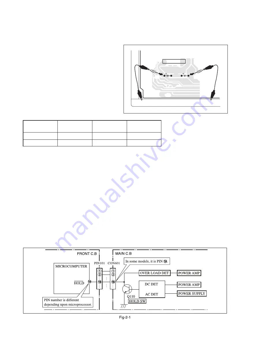
1. Forced discharge of electrolytic capacitor of power supply block
When repair is going to be attempted in the set that uses relay circuit in the power supply block, electric potential is kept charged across
the electrolytic capacitors (C101, 102) even though AC power cord is removed. If repair is attempted in this condition, secondary defect
can occur.
In order to prevent the secondary trouble, perform the following measures before starting repair work.
Discharge procedure
1
1
1
1
1
Remove the AC power cord.
2
2
2
2
2
Connect a discharging resistor at an end of lead wire that
has clips at both ends. Connect the other end of the lead
wire to metal chassis.
3
3
3
3
3
Contact the other end of the discharging resistor to the
positive (+) side (+VH) of C101. (For two seconds)
4
4
4
4
4
Contact the same end of the discharging resistor as step
3
3
3
3
3
to the negative (-) side (-VH) of C102 in the same way.
(For two seconds)
5
5
5
5
5
Check that voltage across C101 and C102 has decreased
to 1 V or less using a multimeter or an oscilloscope.
Select a discharging resistor referring to the following table.
Fig-1
MAIN C.B
D101
C101
C102
2
2
3
4
Summary of Contents for XR-DV826
Page 13: ... 13 BLOCK DIAGRAM 1 DVD MAIN ...
Page 14: ... 14 BLOCK DIAGRAM 2 MAIN FRONT MIC AMP IF AMP PROLOGIC PT DECK ...
Page 16: ... 16 SCHEMATIC DIAGRAM 1 MAIN 1 4 AMP SECTION VM3 ...
Page 17: ... 17 SCHEMATIC DIAGRAM 2 MAIN 2 4 TUNER SECTION TO MAIN C B 1 4 AMP SECTION 1A 13A ...
Page 18: ... 18 SCHEMATIC DIAGRAM 3 MAIN 3 4 DECK SECTION HEAD 1 HEAD 2 ...
Page 19: ... 19 SCHEMATIC DIAGRAM 3 MAIN 4 4 PRO LOGIC SECTION ...
Page 22: ... 22 SCHEMATIC DIAGRAM 5 FRONT CD KEY MIC DECK ...
Page 26: ... 26 SCHEMATIC DIAGRAM 6 AMP 1F ...
Page 28: ... 28 SCHEMATIC DIAGRAM 7 AMP PROLOGIC ...
Page 30: ... 30 SCHEMATIC DIAGRAM 8 PT ...
Page 32: ... 32 FL BJ789GNK GRID ASSIGINMENT ANODE CONNECTION PIN CONNECTION ...
Page 33: ... 33 IC BLOCK DIAGRAM ...
Page 34: ... 34 ...
Page 35: ... 35 ...


