background image

48

1

2

3

4

5

6

7

8

9

10

11

12

13

14

15

16

17

18

19

20

21

22

23

24

25

26

27

28

29

30-42

43-45

46

47-50

51

52-63

64

65

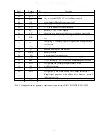
IC, LC876564

Pin No.

Pin Name

I/O

Description

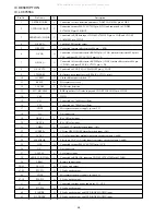
IC DESCRIPTION

_______________

I-STEREO/DRF

I-TUDO/I-SQOUT

I-RDSDATA/O-COIN

___________

O-F.LED

O-M.STB

O-CLK

O-DATA

O-VOLCTL

I-TMBASE

_____________

O-CKSFT

RESET

I-ACOFF

I-TU-SIG/I-MS

VSS

CF1

CF2

VDD1

N.C

I-KEY1

I-KEY0

I-DSW

I-CDTSW

I-ENC1

M SENSOR

O-CE

N.C.

I-LEVEL

I-RDS-CLK/I-WRQ

I-RMC

G1-G13

P33-P35

VDD3

P29-P32

VP

P17-P28

________

P16/BBE

______________

P15/DOLBY

I

I

I

O

O

O

O

O

I

O

I/O

I

I

I

I

I

I

I

I

O

I

I

I

O

O

O

O

O

O

Connected to stereo detection and tuner CD ASP LA9241ML pin-54 DRF.

Connected to tuner PLL IC LC72131 pin-

6

 DO and connected  to CD DSP

LC78622ED pin-55 SQOUT.

Connected to RDS data input CD DSP LC78622ED pin-56 COIN and CD ASP

LA9241ML pin-52 DAT.

Function LED control output.

Connected to main shift resistor 4094 pin-

1

 STB.

Connected to front shift resistor BU2092 pin-

3

 CLK, main shift resistor 4094 pin-

3

CLK, and tuner PLL IC LC72131 pin-

5

 CL.

Connected to front shift resistor BU2092 pin-

2

 DATA, main shift resistor 4094 pin-

2

 DATA, and tuner PLL IC LC72131 pin-

4

 DI.

Connected to VOL/P.EQ IC M62439SP pin-

!

 CONT.

Reference clock input for clock PLL IC LC72131 pin-

7

.

Clock shift output is shifted: “L”

Microprocessor reset.

Hold status detection.

RDS signal level AD value input, and CD ASP LA9241ML pin-52 DAT.

GND.

Connected to 5.76 MHz oscillator

Connected to 5.76 MHz oscillator.

Microprocessor power supply. (µ-com 5 V)

Not connected.

Key AD value input.

Key AD value input.

Deck MECA status detection input. (AD)

CD tray OPEN/CLOSE status detection input. (AD)

AD value input from multiple jog rotary encoder outputs A and B.

Electronic VOL’s AD value input from rotary encoder outputs A and B.

Connected to tuner PLL IC LC72131 pin-

3

 CE.

Not connected.

Level meter input.

Connected to RDS CLK input and CD DSP LC78622ED pin-53 WRQ.

Remote control input.

FL tube grid output.

FL tube anode output.

Microprocessor power supply. (µ-com 5 V)

FL tube anode output.

Connected to minus power supply for FL, -VFL.

FL tube anode output.

FL tube anode output, and INT.DIODE MATRIX input.

FL tube anode output, and INT.DIODE MATRIX input.

All manuals and user guides at all-guides.com

Summary of Contents for XR-M77K

Page 1: ...STEM XR M78 XR M77 S M Code No 09 995 331 7R2 EZ K SERVICE MANUAL REVISION D A T A This Service Manual is the Revision Publishing and replaces Simple Manual S M Code No 09 995 331 7T2 All manuals and user guides at all guides com a l l g u i d e s c o m ...

Page 2: ... 3 CD INSERTED PARTS 23 24 WIRING 4 CD CHIP PARTS 25 26 WIRING 5 FRONT 27 28 SCHEMATIC DIAGRAM 3 FRONT 29 30 WIRING 6 TUNER 31 32 SCHEMATIC DIAGRAM 4 TUNER 33 34 WIRING 7 PT INSERTED PARTS 35 36 WIRING 8 PT CHIP PARTS 37 38 SCHEMATIC DIAGRAM 5 PT 39 40 WIRING 9 MECHA 41 VOLTAGE CHART 42 44 ELECTRICAL ADJUSTMENT 45 47 PRACTICAL SERVICE FIGURE 47 IC DESCRIPTION 48 53 IC BLOCK DIAGRAM 54 55 MECHANICA...

Page 3: ...RC ZAT04 VS SPECIFICATIONS Design and specifications are subject to change without notice Dolby noise reduction manufactured under license from Dolby Laboratories Licensing Corporation DOLBY and the double D symbol are trademarks of Dolby Laboratories Licensing Corporation The word BBE and the BBE symbol are trademarks of BBE Sound Inc Under license from BBE Sound Inc All manuals and user guides a...

Page 4: ...entraîner une dangereuse exposition aux radiations ADVARSEL Usynlig laserståling ved åbning når sikkerhedsafbrydereer ude af funktion Undgå udsættelse for stråling This Compact Disc player is classified as a CLASS 1 LASER product The CLASS 1 LASER PRODUCT label is located on the rear exterior This set employs laser Therefore be sure to follow carefully the instructions below when servicing WARNING...

Page 5: ...2 50 7L C557 87 015 692 080 CAP E 0 22 50 7L C558 87 015 692 080 CAP E 0 22 50 7L C561 87 015 680 080 CAP E 47 10 7L C562 87 015 680 080 CAP E 47 10 7L C563 87 010 154 080 CAP CHIP 10P C565 87 015 688 080 CAP E 4 7 35 7L C566 87 015 688 080 CAP E 4 7 35 7L C567 87 015 679 080 33U 10V SRA C568 87 015 679 080 33U 10V SRA C585 87 015 695 080 CAP E 1 50 7L C586 87 015 695 080 CAP E 1 50 7L C804 87 010...

Page 6: ... 010 312 080 C CAP S 15P 50 CH C445 87 010 196 080 CHIP CAPACITOR 0 1 25 C446 87 010 196 080 CHIP CAPACITOR 0 1 25 C447 87 010 196 080 CHIP CAPACITOR 0 1 25 C448 87 010 315 080 C CAP S 27P 50 CH C450 87 012 140 080 CAP 470P C451 87 012 156 080 C CAP S 220P 50 CH C453 87 010 322 080 C CAP S 100P 50 CH C455 87 010 060 080 ELECTROLYTIC 100 16V C457 87 010 316 080 C CAP S 33P 50 CH C458 87 010 316 080...

Page 7: ...R 0 1 25 C728 87 010 248 080 CAP ELECT 220 10V C729 87 012 274 080 CHIP CAP U 1000P 50B C731 87 012 286 080 CAP U 0 01 25 C733 87 012 280 080 CAP U 3300P 50 C734 87 012 280 080 CAP U 3300P 50 C752 87 012 282 080 CAP U 4700P 50 C753 87 012 195 080 C CAP U 100P 50CH C755 87 012 286 080 CAP U 0 01 25 C756 87 012 286 080 CAP U 0 01 25 C757 87 012 188 080 C CAP U 47P 50 CH C758 87 012 167 080 C CAP U 5...

Page 8: ...IL 1 POLE MPX TOK L832 87 005 847 080 COIL 2 2UH CECS L851 87 005 847 080 COIL 2 2UH CECS EZ L941 87 A50 020 010 COIL ANT LW COI L942 87 A50 019 010 COIL OSC LW COI L981 8Z ZA1 665 010 COIL AM PACK 2 TOK TC942 87 011 164 010 CAPACITOR TRIMMER 30P X721 87 A70 061 010 VIB XTAL 4 500MHZ CSA 309 X851 87 A70 091 010 VIB XTAL 4 332MHZ CSA 309 EZ Regarding connectors they are not stocked as they are not ...

Page 9: ...TRATION ECB PE8050 PE8550 ECB 2SC1815 ECB 2SA933 2SB1370 B E C 2SA1162 2SC2712 DTA114YK DTA144EK DTC114EK DTC114TK DTC114YK BCE FL 13 ST 36GNAK GRID ASSIGNMENT ANODE CONNECTION All manuals and user guides at all guides com ...

Page 10: ...12 11 BLOCK DIAGRAM 1 TO TUNER ADAPTOR PWB RL881B All manuals and user guides at all guides com ...

Page 11: ...14 13 BLOCK DIAGRAM 2 All manuals and user guides at all guides com a l l g u i d e s c o m ...

Page 12: ...16 3 5 1 1 1 16 15 14 13 2 1 1314 16 16 14 13 15 1 2 1 1 14 6 5 5 9 6 13 TO FROM FRONT C B WH201 TO FROM CD C B CN405 TO FROM PT C B WH501 TO FROM CD C B CN804 TO FROM PT C B CN8801 TO FROM PT C B WH803 TO FROM TUNER C B CN701 TO FROM FRONT C B WH204 1 3 CN803 J801 PHONES L R L R _ EZ MODEL EZ MODEL CN204 All manuals and user guides at all guides com ...

Page 13: ...1 2 3 4 5 6 7 8 9 10 11 12 13 14 A B C D E F G H I J K 18 17 WIRING 2 MAIN CHIP PARTS TUNER ADAPTOR C B MAIN C B All manuals and user guides at all guides com ...

Page 14: ...B WH204 TO FROM PT C B CN8801 TO FROM CD C B CN804 TO FROM PT C B WH803 TO FROM FRONT C B WH201 TO FROM CD C B CN405 MAIN C B PHONES CN201 R R 16 4 7 35 25 25 0 068 0 068 0 22 50 35 C844 100p C843 100p 1 2 3 4 5 CN204 SIG MS RD DATA RD CLK NC DGND EZ MODEL All manuals and user guides at all guides com ...

Page 15: ...TAL OUT C B 2SC2712 2SC2712 2SC2712 2SA1162 2SC2712 DIGITAL OUT LED DRIVER Q815 817 VF REG Q809 810 AC DETECT MOTOR LOAD PROTECT Q471 REG PROTECT 2SC2712 2SC2712 B SWITCH SWITCH SLED SPIN MOTOR DRIVE 16 16 R CURRENT LIMITER 6 3 16 16 CN401 100p 16 APC 2SA933 SFR401 R4491 22 R4492 22 R4493 22 R4494 22 C478 470 10 IN4148 L403 BL01RN1 All manuals and user guides at all guides com ...

Page 16: ...TO FROM PICK UP ASSY TO FROM FRONT C B WH401 TO FROM MOTOR C B TO FROM MAIN C B WH804 TO FROM MAIN C B WH405 TO FROM FRONT C B CN205 TO FROM DIGITAL OUT C B WH404 1 1 1 1 1 6 1 6 2 1 2 1 16 17 32 6 16 18 M M1 LOADING S1 OPEN S2 CLOSE CN404 All manuals and user guides at all guides com a l l g u i d e s c o m ...

Page 17: ...1 2 3 4 5 6 7 8 9 10 11 12 13 14 A B C D E F G H I J K 26 25 WIRING 4 CD CHIP PARTS CD C B CONTROL C B All manuals and user guides at all guides com ...

Page 18: ... H I J A B C D E F G H I J FRONT C B CONDUCTOR SIDE TO FROM CONTROL C B WH203 TO FROM CD C B CN401 FRONT C B COMPONENT SIDE TO FROM MAIN C B CN201 1 5 1 5 WH204 TO FROM MAIN C B CN204 EZ MODEL D205 D202 LW RDS EZ MODEL All manuals and user guides at all guides com ...

Page 19: ...OL C B LED DRIVER BUFFER DECODER 2 2 50 0 47 50 LED DRIVER DRIVER SW R R R R R SW SW SYSTEM D202 205 IN4148 P12 P09 LW D205 D202 RDS RECIVER 16 330 6 3 220 10 16 REG RESET TO FROM MAIN C B CN204 1 2 3 4 5 WH204 SIG MS RD DATA RD CLK NC GND EZ MODEL EZ MODEL R2209 1k R02 R01 R03 R2204 1k R2205 1k R03 R02 R01 EZ MODEL EZ MODEL EZ MODEL D219 DAN202K All manuals and user guides at all guides com ...

Page 20: ...32 31 WIRING 6 TUNER 1 2 3 4 5 6 7 8 9 10 11 12 13 14 A B C D E F G H I J K TO FROM TUNER ADAPTOR C B WH102 All manuals and user guides at all guides com ...

Page 21: ...A AM TRACKING ADJ BAND SW IF AMP AM IF ADJ DC BALANCE FM AM TUNER IF STEREO SYSTEM TP6 TP5 TUNER ON OFF SW CN701 TUNER C B SIGNAL FM AM T1 TO FROM TUNER ADAPTOR C B WH102 All manuals and user guides at all guides com a l l g u i d e s c o m ...

Page 22: ... A B C D E F G H I J K PT C B DIGITAL OUT C B TO FROM MAIN C B CN801 TO FROM CD C B CN404 9 1 PT881 3 1 TO FROM MAIN C B CN803 TO FROM MAIN C B CN501 1 9 1 4 5 8 PT882 J502 MD IN AUX IN LINE OUT L R LED902 DIGITAL OUT 1 6 All manuals and user guides at all guides com ...

Page 23: ...38 37 WIRING 8 PT CHIP PARTS 1 2 3 4 5 6 7 8 9 10 11 12 13 14 A B C D E F G H I J K PT C B DIGITAL OUT C B 230V 50Hz All manuals and user guides at all guides com ...

Page 24: ...ROM MAIN C B CN803 TO FROM MAIN C B CN501 TO FROM MAIN C B CN801 PT C B 63MA 250V 230V 50Hz POWER OFF DISCHARGE MUTE MUTE MUTE MUTE DRIVE MUTE DRIVE LINE AMP 2S L501 BL01RN1 3 3 50 DTA114YK All manuals and user guides at all guides com ...

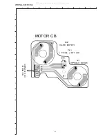
Page 25: ...41 1 2 3 4 5 6 7 A B C D E F G H I J K WIRING 9 MECHA MOTOR C B TO FROM CD C B CN403 All manuals and user guides at all guides com ...

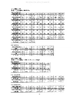
Page 26: ...42 VOLTAGE CHART All manuals and user guides at all guides com a l l g u i d e s c o m ...

Page 27: ...43 All manuals and user guides at all guides com ...

Page 28: ...44 All manuals and user guides at all guides com ...

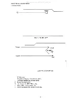
Page 29: ...45 ELECTRICAL ADJUSTMENT CD SECTION All manuals and user guides at all guides com ...

Page 30: ...46 8 3 7 L771 L772 TP1 4 L981 FFE801 TP2 R785 30 IC771 TP4 TP3 TP6 GND TP5 CN701 12 11 10 TUNER C B 4 6 L942 L941 TC942 7 TUNER SECTION All manuals and user guides at all guides com ...

Page 31: ...kHz 4 MW Tracking Adjustment Settings Test point TP5 TP6 Adjustment location L981 Method Set to MW 999kHz and adjust L981 so that the test point becomes maximum 5 FM VT Check Settings Test point TP1 VT Method Set to FM 87 5MHz 108 0MHz and check that the test point is more than 0 5V 87 5MHz and less than 8 0V 108 0MHz 6 LW VT Adjustment Settings Test point TP2 VT Adjustment location L942 Method Se...

Page 32: ...L IC LC72131 pin 5 CL Connected to front shift resistor BU2092 pin 2 DATA main shift resistor 4094 pin 2 DATA and tuner PLL IC LC72131 pin 4 DI Connected to VOL P EQ IC M62439SP pin CONT Reference clock input for clock PLL IC LC72131 pin 7 Clock shift output is shifted L Microprocessor reset Hold status detection RDS signal level AD value input and CD ASP LA9241ML pin 52 DAT GND Connected to 5 76 ...

Page 33: ...INT DIODE MATRIX input Microprocessor power supply µ com 5 V FL tube anode output SHOP Deck mechanism status detection input CAM Deck mechanism status detection input AUTO Q surround IC control output Key scan detection timing switch Deck mechanism motor control output Connected to front shift resistor IC BU2092 pin 5 CD tray open control output CD tray close control output Power supply ON OFF con...

Page 34: ...ween the TD and VR pins Tracking phase compensation setting pin Tracking jump signal kick pulse amplitude setting pin Tracking control signal output pin Focusing control signal output pin Pin to which external focusing phase compensation constants are connected between the FD and FA pins Pin to which external focusing phase compensation constants are connected between the FD and FA pins Pin to whi...

Page 35: ...GND Output pin to which external focus search smoothing capacitor is connected Tracking Balance Control EF balance variable range setting pin No connection Disc defect detector output pin Reference clock input pin 4 23 MHz of the DSP is input Microprocessor command clock input pin Microprocessor command data input pin Microprocessor command chip enable input pin Detect RF RF level detector output ...

Page 36: ...hmidt input Tracking error signal input pin Schmidt input Tracking OFF output pin Tracking gain selection output pin Gain boost at L Track jump control signal output pin Three level output is possible using command EFM data playback clock monitoring pin 4 3218 MHz when phase is locked in Sync signal detection output pin H when the sync signal which is detected from EFM signal and thesync signal wh...

Page 37: ...l which is generated by dividing frequency of crystal oscillator Subcode Q output standby output pin Read write control input pin Schmidt input Subcode Q output pin Command input pin from microprocessor Command input read clock or subcode read input clock from SQOUT pin LC78622 reset input pin Set this pin to L once when the main power is turned on Test signal output pin Use this pin as open norma...

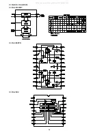
Page 38: ...54 IC BLOCK DIAGRAM IC BU4094BCF IC BA3880FS IC BU2092 All manuals and user guides at all guides com ...

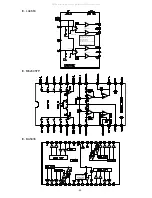
Page 39: ...L OUTPUT AMP OUTPUT AMP INPUT AMP INPUT AMP POWER GND SHORTING PROTECT CIRCUIT LOAD SHORTING PROTECT CIRCUIT THERMAL PROTECTION CIRCUIT PROTECTION CIRCUITS IC LA4663 IC M62495FP IC BA5936 All manuals and user guides at all guides com ...
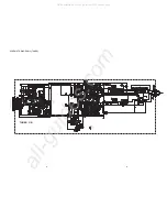
Page 40: ...29 8Z CL5 210 010 CHAS CD 30 8Z CL5 005 010 LID CD 31 8Z CL5 008 010 WINDOW CD 32 8Z CL5 003 010 CABI SIDE R 33 8Z CL5 683 010 PT E 34 8Z CL5 213 010 HLDR A PWB TU 35 8Z CL5 216 010 FOOT CABI 36 8Z CLF 010 010 CABI REAR E 37 8Z CL5 004 010 CABI SIDE L 38 87 085 185 010 BUSHING AC CORD E 39 8Z NB8 240 010 COVER PL 40 8Z CL5 221 010 HLDR BKT MOUNT 41 8Z CL5 622 010 F CABLE 9P 2 5 250MM UL2468 AW 42 ...

Page 41: ...3 46 29 31 30 32 P C B 33 56 40 39 41 37 P C B P C B P C B HS BKT 38 TUNER BRACKET 35 36 42 43 44 45 34 48 54 FIBRE PLATE C C D P C B A A A A A A A A D D D D D D C E K C D D CHAS BOTTOM B A A A L HT SINK F N J G 24 52 E E E H E K E M H O K K E 21 MOTOR I I 25 50 49 C G SH DFSR LED All manuals and user guides at all guides com a l l g u i d e s c o m ...

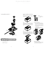
Page 42: ...move the panel Turn the speaker unit to counter clockwise direction while inserting a flat bladed screwdriver into one of the hollows arround speaker unit and then remove the speaker unit After replacing the speaker unit install it turnning to clock wise direction unitil click sound comes out Type 1 Type 3 Type 2 TOOLS 1 Plastic head hammer 2 flat head screwdriver 3 Cut chisel How to Remove the PA...

Page 43: ...NO SPEAKER PARTS LIST 1 1 1 8Z CL5 543 010 CORD SP 2 8Z CL5 506 010 GRILLE FRAME ASSY 3 8Z CL5 503 010 PANEL FR 4 8Z CL5 505 010 PANEL TW 5 8Z CL5 542 010 SPKR TW25 6 8Z CL5 541 010 SPKR W100 All manuals and user guides at all guides com ...
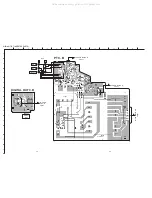
Page 44: ...737004 Printed in Singapore 2 11 IKENOHATA 1 CHOME TAITO KU TOKYO 110 8710 JAPAN TEL 03 3827 3111 All manuals and user guides at all guides com ...

Reviews: