– 52 –
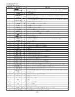
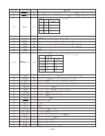
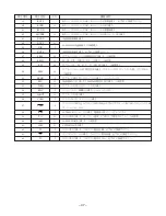
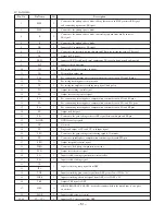
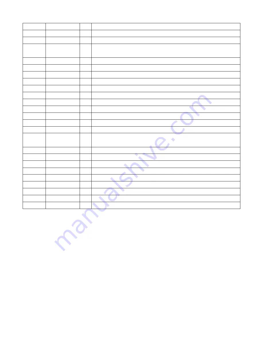
41
RFSM
O
Output for RF.
42
RFS–
O
For setting RF gain and 3T compensation constant together with RFSM.
43
SLC
O
SLICE LEVEL CONTROL; output for controlling the data slice level of DSP with
RF waveform.
44
SLI
I
Input for controlling the data slice level of DSP.
45
D-GND
–
GND for digital system.
46
FSC
O
Output pin for focus search smoothing capacitor.
47
TBC
I
(Tracking Balance Control) EF balance variable range setting pin.
48
NC
–
Not connected.
49
DEF
O
Output for disk defect detection.
50
CLK
I
Standard clock input; DSP's 4.23MHz is inputted.
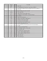
51
CL
I
Clock input for microcontroller command.
52
DAT
I
Data input for microcontroller command.
53
CE
I
Chip-enable input for microcontroller command.
54
DRF
O
Detect RF; output for RF level detection.
55
FSS
I
(Focus Search Mode) = search against reference voltage switching pin.
(Not used)
56
VCC2
–
VCC pin for servo and digital systems.
57
REFI
I
For connecting pass capacitor to reference voltage.
58
VR
O
Reference voltage output.
59
LF2
–
For setting disk defect-detection time constant.
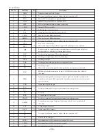
60
PHI
–
Connects to capacitor for RF signal peak hold.
61
BHI
–
Connects to capacitor for RF signal bottom hold.
62
LDD
O
Output for APC circuit.
63
LDS
I
Input for APC circuit.
64
VCC1
–
VCC pin for RF system.
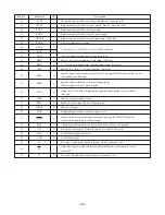
Pin No.
Pin Name
I/O
Description
Summary of Contents for XR-MD510
Page 5: ... 5 ...
Page 15: ... 15 SCHEMATIC DIAGRAM 1 MAIN PT1 PT2 RELAY ...
Page 17: ... 17 SCHEMATIC DIAGRAM 2 FRONT SW 1 SW 2 FACE A FACE B FACE C DECK ...
Page 20: ... 20 SCHEMATIC DIAGRAM 3 CD CD LOAD CD DRIVE ...
Page 22: ... 22 SCHEMATIC DIAGRAM 4 D TUNER ...
Page 24: ... 24 SCHEMATIC DIAGRAM 5 K TUNER ...
Page 26: ... 26 SCHEMATIC DIAGRAM 6 EZ TUNER ...
Page 29: ... 29 IC BLOCK DIAGRAM IC BA5936S IC BU2099FV ...
Page 30: ... 30 IC BU2092F IC BU1920FS ...
Page 31: ... 31 IC MM1454XFBE IC LA1837NL ...
Page 32: ... 32 IC TA2040AF IC HA12211 ...
Page 33: ... 33 IC CXA1553P IC LC72131D ...
Page 34: ... 34 IC BD3876KS2 ...
Page 38: ... 38 8 SFR130 TP3 VREF TP2 FE C CD C B L201 7 TP1 K SCAN GND IC201 7 B FRONT C B ...
Page 43: ... 43 98 O ARDY O 99 O SREQ O 100 I MREQ I ja ja 01234 ja 0123 fLl ...
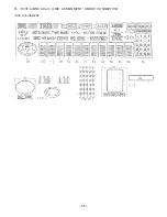
Page 55: ... 55 FL 13 ST 44GNK ACJ 4 GRID ASSIGNMENT ANODE CONNECTION GRID ASSIGNMENT ...
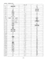
Page 56: ... 56 ANODE CONNECTION ...

