background image

– 54 –

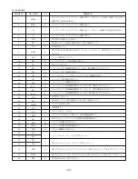
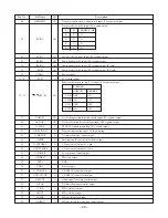
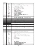
38

LVSS

Left channel one-bit D/A converter ground. Must be connected to 0V.

39

RVSS

Right channel one-bit D/A converter ground. Must be connected to 0V.

40

RCHO

O

Right channel one-bit D/A converter output.

41

RVDD

Right channel one-bit D/A converter power supply.

42

MUTER

O

Right channel one-bit D/A converter mute ouput. (Not used)

43

XVDD

Crystal oscillator power supply.

44

XOUT

O

Connections for a 16.934MHz crystal oscillator element.

45

XIN

I

46

XVSS

Crystal oscillator ground. Must be connected to 0V.

47

SBSY

O

Subcode block synchronization signal output. (Not used)

48

EFLG

O

C1, C2 single and double error correction monitor pin. (Not used)

49

PW

O

Subcode P, Q, R, S, T, U, V and W output. (Not used)

50

SFSY

O

Subcode frame synchronization signal output. This signal falls when the subcode are in

the standby state. (Not used)

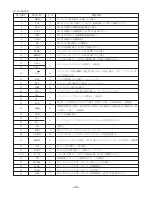
51

SBCK

I

Subcode readout clock input. This is a Schmitt input.

(Must be connected to 0V when unused)

52

FSX

O

Output for the 7.35 kHz synchronization signal divided from the crystal oscillator.

(Not used)

53

WRQ

O

Subcode Q output standby output.

54

RWC

I

Readwrite control input. This is a Schmitt input.

55

SQOUT

O

Subcode Q output.

56

COIN

I

Command input from the control microprocessor.

57

CQCK

I

Input for both the command input acquisition clock and the SQOUT pin subcode

readout clock input. This is a Schmitt input.

58

RES

I

Chip reset pin. This pin must be set low briefly after power is first applied.

59

T11

O

Test output. Leave open. (Normally outputs a low level). (Not used)

60

16M

O

16.9344 MHz output. (Not used)

61

4.2M

O

4.2336 MHz output.

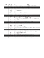
62

T5

I

Test input. A pull-down resistor is built in. Must be connected to 0V.

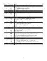
63

CS

I

Chip select input. A pull-down resistor is built in. Must be connected to 0V if not

controlled.

64

T1

I

Test input. No pull-down resistor. Must be connected to 0V.

Pin No.

Pin Name

I/O

Description

Summary of Contents for XR-MD510

Page 1: ...MMNJPQNJOkNF DISASSEMBLY INSTRUCTION CD TEST MODE 0 This Service Manual is the Revision Publishing and replaces Simple Manual XR MD510 511 K EZ S M Code No 09 002 422 8T2 If requiring information about the MD mechanism see Service Manual of AZG 4A S M Code No 09 001 341 2N2 This Service Manual does not include DISASSEMBLY INSTRUCTION and TEST MODE These items will be issued in the next Supplement ...

Page 2: ...AM 3 CD CD LOAD CD DRIVE 20 WIRING 5 D TUNER 21 SCHEMATIC DIAGRAM 4 D TUNER 22 WIRING 6 K TUNER 23 SCHEMATIC DIAGRAM 5 K TUNER 24 WIRING 7 EZ TUNER 25 SCHEMATIC DIAGRAM 6 EZ TUNER 26 WIRING 8 DECK RELAY 27 WIRING 9 PT1 PT2 28 IC BLOCK DIAGRAM 29 34 ADJUSTMENT TUNER DECK FRONT CD 35 40 IC DESCRIPTION 41 54 FL 13 ST 44GNK ACJ 4 GRID ASSIGNMENT ANODE CONNECTION 55 56 MECHANICAL EXPLODED VIEW 1 1 57 M...

Page 3: ...mb hbop S melkbp PO Q O RM NSMMMeò RM NRMMMeò a a a a a NÄáí j a j a j a j a j a QMM VMMêéã is QQKNâeò POâeò QQKNâeò QUâeò O N bcj La La La La La aL aL aL aL aL NÄáí OM OMIMMMeò MKR NKRÇ_ MKMMN tKmb h NMMs RMLSMeò SRt NTR ORT PPP ãã SKRâÖ O bf gF S USÇ_LtLã NPÅã OKOÅã NRR ORQ ONM ãã OKShÖ 012 3 __b __b __b __b 012345678 I ali_v a h SPECFICATIONS D ...

Page 4: ... nm D A converter 1 bit dual Signal to noise ratio 85 dB 1 kHz 0 dB Harmonic distortion 0 05 1 kHz 0 dB Wow and flutter Unmeasurable SPECIFICATIONS K EZ MD recorder section Scanning method Non contact optical scanner Semiconductor laser application Recording system Magnetic polarity modulation overwrite system Rotation speed Approx 400 to 900 rpm CLV Sampling frequency 44 1kHz No of channels Stere...

Page 5: ... 5 ...

Page 6: ...ceras i denna bruksanvising kan användaren utsättas för osynling laserstrålning som överskrider gränsen för laserklass 1 PROTECTION OF EYES FROM LASER BEAM DURING SERVICING CAUTION Use of controls or adjustments or performance of proce dures other than those specified herin may result in hazardous radiation exposure ATTENTION L utillisation de commandes réglages ou procédures autres que ceux spéci...

Page 7: ...E DAN217 87 A40 488 080 0E DIODE 1SS244 87 020 465 010 0E DIODE 1SS133 110MA 87 A40 437 080 ZENER MTZJ4 3B 87 A40 002 080 0E ZENER MTZJ5 1C 87 A40 234 080 0E ZENER MTZJ5 6A 87 017 932 080 0E ZENER MTJ6 2B 87 070 136 080 0E ZENER MTZJ5 1B 87 017 149 080 0E ZENER HZS6A2L MAIN C B C102 87 016 051 000 1B CAP E 2200 35 M SMG D C103 87 016 051 000 1B CAP E 2200 35 M SMG D C104 87 012 368 080 0E C CAP S ...

Page 8: ...010 380 080 0E CAP E 47 16 M 11L SME C401 87 010 401 080 CAP ELECT 1 50V K EZ C402 87 010 263 080 CAP ELECT 100 10V K EZ C403 87 010 260 080 CAP ELECT 47 25V K EZ C410 87 010 260 080 CAP E 47 25 M 11L SME K EZ C461 87 010 402 080 0E CAP ELECT 2 2 50V C462 87 010 400 080 0E CAP ELECT 0 47 50V C491 87 010 404 080 0E CAP ELECT 4 7 50V C492 87 010 404 080 0E CAP ELECT 4 7 50V C501 87 010 374 080 0E CA...

Page 9: ...A401 88 802 092 420 1B CONN ASSY 9P FC102 8A CJ4 645 010 FF CABLE 17P 1 0 FL301 8A CJ4 604 010 FL 13 ST 44GNK ACJ 4 L201 87 A50 333 010 0E COIL OSC 9 43MHZ LED151 87 A40 317 080 0E LED SLR 342VCT31 RED LED152 87 A40 317 080 0E LED SLR 342VCT31 RED LED153 87 A40 317 080 0E LED SLR 342VCT31 RED LED154 87 A40 317 080 0E LED SLR 342VCT31 RED LED155 87 A40 317 080 0E LED SLR 342VCT31 RED LED156 87 A40 ...

Page 10: ...CAP S 0 01 25 KB C829 87 010 197 080 0E C CAP S 0 01 25 KB C830 87 010 197 080 0E C CAP S 0 01 25 KB C831 87 010 197 080 0E C CAP S 0 01 25 KB C834 87 010 197 080 0E C CAP S 0 01 25 KB C835 87 010 197 080 0E C CAP S 0 01 25 KB CN801 87 A60 621 010 0E CONN 4P V 2MM JMT CNA301 8A CJ4 644 010 CONN ASSY 9P H PANEL CNA802 8A CJ4 643 010 CONN ASSY 4P V FACE C D831 87 A40 496 040 0E LED SLR 342MCT31 GRN ...

Page 11: ...6 080 0E CAP U 0 01 25 C766 87 010 197 080 C CAP S 0 01 25 KB EZ K C768 87 012 286 080 0E CAP U 0 01 25 C769 87 010 260 080 0E CAP ELECT 47 25V C770 87 010 829 080 0E CAP U 0 047 16 C771 87 010 383 080 0E CAP ELECT 33 25V C772 87 010 829 080 0E CAP U 0 047 16 C773 87 010 196 080 0E CHIP CAPACITOR 0 1 25 C774 87 010 263 080 0E CAP ELECT 100 10V C775 87 010 404 080 0E CAP ELECT 4 7 50V C776 87 012 2...

Page 12: ... 010 FLTR CF SFE10 7MS3G A EZ K CF802 87 008 261 010 1A FILTER SFE10 7MA5 A D CF802 82 785 747 010 CF MS2 GHY R EZ K CN701 87 A60 700 010 0E CONN 13P H GRY TUC P13X C1 D K CN701 87 A60 650 010 CONN 16P H GRY TUC P16X C1 EZ FFE801 A8 6ZA 19A 070 6ZA 1 FEJNC D FFE801 A8 6ZA 191 130 6ZA 1 FEENM EZ K J801 87 A60 702 010 1B TERMINAL ANT 4P CJ 9036 D J801 87 033 241 010 TERMINAL ANT 2P AJ 2039 EZ K L771...

Page 13: ...1344 2SB1370 2SB1625 2SD2025 2SD2494 2SA1318 CSD655 2SC4115 2SA933 E C B E C B E B C 2SA1235 2SC2714 2SC3052 2SD1306 CMBT5401 CMBT5551 CSD1306 DTA123EKA DTA123JK DTA143EK D G S 2SK543 4 5 S G D 2SJ461 T1 2SK2158 DTA144TK DTC114EK DTC114TK KTA1298 RT1N141C RT1N144C RT1P141C RT1P144C RT1P441C ...

Page 14: ...WIRING 1 MAIN 14 10 11 12 13 14 15 16 17 18 19 20 21 22 23 24 A B C D E F G H I J K L M N O P Q R S T U 1 2 3 4 5 6 7 8 9 25 26 27 28 29 30 31 32 ...

Page 15: ... 15 SCHEMATIC DIAGRAM 1 MAIN PT1 PT2 RELAY ...

Page 16: ...WIRING 2 FRONT SW 1 SW 2 16 10 11 12 13 14 15 16 17 18 19 20 21 22 23 24 A B C D E F G H I J K L M N O P Q R S T U 1 2 3 4 5 6 7 8 9 25 26 27 28 29 30 31 32 ...

Page 17: ... 17 SCHEMATIC DIAGRAM 2 FRONT SW 1 SW 2 FACE A FACE B FACE C DECK ...

Page 18: ...WIRING 3 FACE A FACE B FACE C 18 10 11 12 13 14 15 16 17 18 19 20 21 22 23 24 A B C D E F G H I J K L M N O P Q R S T U 1 2 3 4 5 6 7 8 9 25 26 27 28 29 30 31 32 ...

Page 19: ...WIRING 4 CD CD LOAD CD DRIVE 19 10 11 12 13 14 15 16 17 18 19 20 21 22 23 24 A B C D E F G H I J K L M N O P Q R S T U 1 2 3 4 5 6 7 8 9 25 26 27 28 29 30 31 32 ...

Page 20: ... 20 SCHEMATIC DIAGRAM 3 CD CD LOAD CD DRIVE ...

Page 21: ...WIRING 5 D TUNER 21 10 11 12 13 14 15 16 17 18 19 20 21 22 23 24 A B C D E F G H I J K L M N O P Q R S T U 1 2 3 4 5 6 7 8 9 25 26 27 28 29 30 31 32 ...

Page 22: ... 22 SCHEMATIC DIAGRAM 4 D TUNER ...

Page 23: ...WIRING 6 K TUNER 23 10 11 12 13 14 15 16 17 18 19 20 21 22 23 24 A B C D E F G H I J K L M N O P Q R S T U 1 2 3 4 5 6 7 8 9 25 26 27 28 29 30 31 32 ...

Page 24: ... 24 SCHEMATIC DIAGRAM 5 K TUNER ...

Page 25: ...WIRING 7 EZ TUNER 25 10 11 12 13 14 15 16 17 18 19 20 21 22 23 24 A B C D E F G H I J K L M N O P Q R S T U 1 2 3 4 5 6 7 8 9 25 26 27 28 29 30 31 32 ...

Page 26: ... 26 SCHEMATIC DIAGRAM 6 EZ TUNER ...

Page 27: ...WIRING 8 DECK RELAY 27 1 2 3 4 5 6 7 8 9 10 11 12 13 14 15 A B C D E F G H I J K L M N O P Q R S T U ...

Page 28: ...WIRING 9 PT1 PT2 28 10 11 12 13 14 15 16 17 18 19 20 21 22 23 24 A B C D E F G H I J K L M N O P Q R S T U 1 2 3 4 5 6 7 8 9 25 26 27 28 29 30 31 32 ...

Page 29: ... 29 IC BLOCK DIAGRAM IC BA5936S IC BU2099FV ...

Page 30: ... 30 IC BU2092F IC BU1920FS ...

Page 31: ... 31 IC MM1454XFBE IC LA1837NL ...

Page 32: ... 32 IC TA2040AF IC HA12211 ...

Page 33: ... 33 IC CXA1553P IC LC72131D ...

Page 34: ... 34 IC BD3876KS2 ...

Page 35: ...Hz TC942 290kHz Method Set up TC942 to center before adjustment The level at 144kHz is adjusted to maximum by L941 Then the level at 290kHz is adjusted to maximum by TC942 6 AM IF Adjustment Settings Test point TP8 Lch TP9 Rch Adjustment location L772 450kHz 7 FM VT Check Settings Test point TP1 VT Method Set to FM 108 0MHz and check that the test point is less than 8 0V Then set to FM 87 5 MHz an...

Page 36: ...EoÅÜF iTTO KKKKKKKKKKKKKKKKKKKKKKKKKKKKKKKKKKKKKKK QRMâeò RK cj sq qmNEsqF cj NMUKMjeò VKMs cj TSKMjeò MKQs SK cj qmUEiÅÜF qmVEoÅÜF cj UPKMjeò UÇ_ TK a L qmP qmQ a qmU qmV iTTN RQÇ_ cj UPKMjeò qmP qmQ Ms MKMQs iTTN NKPB L771 L981 L772 FFE801 1 IC771 TP1 VT TP2 CLK TP4 DC TP3 DC 1 CN701 GND TP8 LCH TP9 RCH TUNER C B D ONLY O 1 2 3 3 4 4 5 6 7 8 9 7 7 36 ...

Page 37: ... 37 SFR351 SFR352 GND TP8 LCH TP9 RCH 5 4 6 1 2 3 SFR304 SFR303 SFR305 SFR306 4 5 6 A MAIN C B DECK R P E HEAD 2 SFR1 CON1 DECK C B K 1 2 ...

Page 38: ... 38 8 SFR130 TP3 VREF TP2 FE C CD C B L201 7 TP1 K SCAN GND IC201 7 B FRONT C B ...

Page 39: ...MQ EoÅÜF OQRãs NMãs pco RK qq JSMO qmU EiÅÜFI qmV EoÅÜF NâeòLNMâeò Eifkb fkF pcoPRN EiÅÜF pcoPRO EoÅÜF Nâeò qmU qmV MÇ_ ENTãsF lp Nâeò NMâeò NMâeò Nâeò MÇ_ MKRÇ_ pco SK qq JSMO qmU EiÅÜFI qmV EoÅÜF Nâeò Eifkb fkF pcoPMR EiÅÜF pcoPMS EoÅÜF Nâeò qmU qmV MÇ_ ENTãsF lp Nâeò MÇ_ MKRÇ_ pco Y TK J lk lp qmN EhJp kF dka iOMN qrkbo afpmi v 0 NVQKUVUeò MKNVQeò iOMN Y a UK q aJTUO qmO EcbFI qmP EsobcF pcoNPM...

Page 40: ...est tape TTA 602 Test point TP8 Lch TP9 Rch Input signal 1kHz 10kHz LINE IN Adjustment location SFR351 Lch SFR352 Rch Method Apply a 1kHz signal and REC mode Then adjust OSC attenuator so that the output level at the TP8 TP9 becomes 0dB 17mV Record and play back the 1kHz and 10kHz signals and adjust SFRs so that the output of the 10kHz signals becomes 0dB 0 5dB with respect to that of the 1kHz sig...

Page 41: ... 23 I ENC1 A D I 24 I ENC0 A D I 25 I LEVEL A D I 26 I SC I MIC A D I 27 I TMBASE I 28 I RDSCLK I I WRQ 29 I RMC I 30 42 G13 G1 O 43 45 P35 P33 O 46 VDD3 47 50 P32 P29 O 51 VP 52 62 P28 P18 O 63 MD P17 I O 64 ECO OFF P16 I O IC DESCRIPTION IC LC87F65C8AU ACJ 4 fLl qr crk a crk a pm f aoc qr crk oap bw a crk a apm f qr crk fc a crk a apm f f f f crk f mii f i e qr crk q mb crk dka EVKQPjeòFK EVKQPj...

Page 42: ...SWA OFF ON SWB ON ON SWC OFF OFF SWD ON ON 79 CAM P2 I O 80 AUTO P1 I O 81 O FUNC O 82 O KEYSCAN O 83 O MOTOR O 84 O FSTB O 85 O CDTOPEN O 86 O CDTCLOSE O 87 O POWER O 88 O MDRST O 89 VSS2 90 VDD2 91 O CD DATA O 92 O CD CLOCK O 93 O MUTE O 94 O SOL O 95 O SIN O 96 I SOUT I 97 I ACLK I 0123 456789ci 01 234567ci O ci N ci P ci O ci Eh F N ci Ebw F ci aJ ci 01 ci ci crk f s e f a e a e ja dka a apm f...

Page 43: ... 43 98 O ARDY O 99 O SREQ O 100 I MREQ I ja ja 01234 ja 0123 fLl ...

Page 44: ...TO O 16 FD O 17 FD I 18 FA O 19 FA I 20 FE O 21 FE I 22 AGND 23 NC 24 SP O 25 SPG I 26 SP I 27 SPD O 28 SLEQ I 29 SLD O 30 SL I 31 SL 32 JP I 33 JP 34 TGL I 35 TOFF I 36 TES O 0cfkN oc cb 0 0c qb 0 qb a qb qb qb qbp qo h boolo pbkpb qb q qa so 01234 5 ca c ca c c cb cb cb qb dka NOÅã pma 0 apm apm 01 2qdiZ e apm 01 2qlccZ e qbp apm ...

Page 45: ...BC I 48 NC 49 DEF O 50 CLK I 51 CL I 52 DAT I 53 CE I 54 DRF O 55 FSS I 56 VCC2 57 REFI 58 VR O 59 LF2 60 PHI 61 BHI 62 LDD O 63 LDS I 64 VCC1 efde cobnrbk v ibsbi apm is oc ocpj oc bcj Pq pif b ibsbi lkqloli oc apm apm 0 12345 dka qê ÅâáåÖ _ ä åÅÉ çåíêçä bc apm QKOPjeò abqb q oc oc s oc oc 0 m m oc s ...

Page 46: ...q bf g 01Ms i N a i i N a i i N a i i N a i Ms 1 DEFI I 2 TAI I 3 PDO O 4 VVSS 5 ISET I 6 VVDD 7 FR I 8 VSS 9 EFMO O 10 EFMIN I 11 T2 I 12 CLV O 13 CLV 14 V P O 15 HFL I 16 TES I 17 TOFF O 18 TGL O 19 JP O 20 JP 21 PCK O 22 FSEQ O 23 VDD 24 SL O 25 SL 26 NC 27 PUIN I 28 CD R W O 29 EMPH O 30 C2F O 31 DOUT O 32 33 T3 T4 I 34 NC 35 MUTEL O 36 LVDD 37 LCHO O 38 LVSS ...

Page 47: ...W O 50 SFSY O 51 SBCK I 52 FSX O 53 WRQ O 54 RWC I 55 SQOUT O 56 COIN I 57 CQCK I 58 RES I 59 T11 O 60 16M O 61 4 2M O 62 T5 I 63 CS I 64 T1 I o N a o Ms o N a o o N a o o N a o NSKVPQjeò Ms 01234 NI OI N O m n o q r t 0123456789 01 2 TKPRâeò n n pnlrq i TUSOOb i i NSKVPQQjeò QKOPPSjeò 01Ms 01 23Ms 0 12Ms ...

Page 48: ...ower supply 18 I ENC2 A D I Waveform input for MD jog rotary encoder 19 I KEY1 A D I Tact key A D level input 20 I KEY0 A D I Tact key A D level input 21 I DSW A D I CD deck RECA B CST switch detection input 22 I CDTSW A D I CD mecha switch detection input 23 I ENC1 A D I Waveform input for jog rotary encoder 24 I ENC0 A D I Waveform input for volume rotary encoder 25 I LEVEL A D I Audio signal le...

Page 49: ...operation detection switch input FL segment output 80 AUTO P1 I O Deck reel rotation detection signal input FL segment output 81 O FUNC O FUNC IC expand port pull up VCC switch output 82 O KEYSCAN O Segment input timing ouput H input timing 83 O MOTOR O Deck mecha motor control output 84 O FSTB O Shift register IC control serial strobe output 85 O CDTOPEN O CD tray control output H open 86 O CDTCL...

Page 50: ... 50 Pin No Pin Name I O Description 99 O SREQ O From MD unit serial data transfer request control output 100 I MREQ I To MD unit serial data transfer request control input ...

Page 51: ...d FA pins 18 FA O For constructing focusing phase compensation constant between FD and FA pins 19 FA I For constructing focusing phase compensation constant between FA and FE pins 20 FE O Output for FE signal 21 FE I Connects to the gain setting resistor of FE signal between this pin and FE pin 22 A GND GND for analog signals 23 NC Not used 24 SP I Single end output of CV and CV pin input signal 2...

Page 52: ... is inputted 51 CL I Clock input for microcontroller command 52 DAT I Data input for microcontroller command 53 CE I Chip enable input for microcontroller command 54 DRF O Detect RF output for RF level detection 55 FSS I Focus Search Mode search search against reference voltage switching pin Not used 56 VCC2 VCC pin for servo and digital systems 57 REFI I For connecting pass capacitor to reference...

Page 53: ...racking gain switching output Increase the gain when low 19 JP O Track jump output 20 JP Three value output is also possible when specified by microprocessor command 21 PCK O EFM data playback clock monitor Outputs 4 3218 MHz when the phase is locked Not used Synchronization signal detection ouput Outputs a high level when the synchronization 22 FSEQ O signal detected from the EFM signal and the i...

Page 54: ...sed 51 SBCK I Subcode readout clock input This is a Schmitt input Must be connected to 0V when unused 52 FSX O Output for the 7 35 kHz synchronization signal divided from the crystal oscillator Not used 53 WRQ O Subcode Q output standby output 54 RWC I Readwrite control input This is a Schmitt input 55 SQOUT O Subcode Q output 56 COIN I Command input from the control microprocessor 57 CQCK I Input...

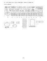
Page 55: ... 55 FL 13 ST 44GNK ACJ 4 GRID ASSIGNMENT ANODE CONNECTION GRID ASSIGNMENT ...

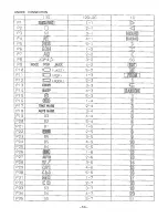
Page 56: ... 56 ANODE CONNECTION ...

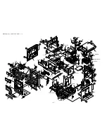
Page 57: ...c a a 1 4 7 2 3 5 6 8 9 P C B P C B P C B 11 13 12 31 15 14 28 17 18 18 20 19 16 23 24 25 26 39 40 FL301 42 35 27 36 37 33 34 32 29 30 3ZG 3 YE3NC P C B P C B P C B P C B 45 46 M901 48 49 63 64 65 56 47 P C B 50 51 53 52 54 59 61 60 62 P C B 44 43 22 41 38 CUSH R 66 21 CHAS MAIN 10 57 2ZM 1 YR9NF PLATE SHLD 58 55 WIRE BINDER AZG 4A HT SINK d d I ...

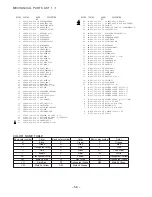
Page 58: ... CABI FR 33 8A CJ4 020 010 KEY JOG EZ 33 8A CJ4 024 010 1C KEY JOG D D K 34 8A CJ4 211 010 1A JOINT CABI 35 8A CJ4 204 010 0E GUIDE LED CONTROL 36 8A CJ4 021 010 1C KEY FUN 37 8A CJ4 029 010 1A REFLECTOR FUN 38 87 085 184 010 0E BUSHING AC CORD D D 38 87 085 185 010 BUSHING AC CORD E EXCEPT D 39 8A CJ4 041 010 1C KEY ASSY POWER 40 8A CJ4 005 010 2A PANEL SIDE L 41 87 050 098 010 1B AC CODE ASSY D ...

Page 59: ...A 8 16 15 14 30 13 12 11 10 17 7 9 19 4 6 20 5 22 21 23 25 42 29 27 28 3 2 P C B HLDR WIRE 3 B B A 14 26 49 A B A B 31 38 39 40 32 34 33 35 43 45 41 41 37 44 24 HLDR MOTOR 18 HLDR IC P C B SOL2 36 47 48 46 C C E CAPSTAN CAPSTAN 2 41 5 D D C C ...

Page 60: ...7 010 0E SPR T CAS 24 82 ZM1 247 210 0E PULLEY MOTOR 25 82 ZM1 242 010 0E LVR CAS 26 82 ZM1 243 010 0E LVR STOP 27 82 ZM1 344 210 0E LVR ASSY PINCH R2 28 82 ZM1 259 210 0E SPR T PINCH R 29 82 ZM1 240 110 0E LVR REC 30 82 ZM1 298 010 0E SPR P EARTH 31 82 ZM1 255 310 0E SPR E LVR DIR 32 82 ZM1 221 310 0E GEAR CAM 33 82 ZM1 227 310 0E LVR TRIG 34 82 ZM1 224 410 0E LVR FR 35 82 ZM1 305 210 0E SPR E TR...

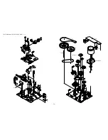
Page 61: ... 61 CD MECHANISM EXPLODED VIEW 1 2 A B C A B C 3 P C B 2 4 5 6 7 8 9 10 11 12 16 14 15 13 1 17 3ZG 2 E3 17 CUSH G MAIN A B C C D D A CUSH G MAIN A ...

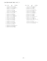
Page 62: ...210 0E GEAR C 8 83 ZG3 205 010 0E GEAR D 9 83 ZG3 217 010 0E S SCREW GEAR D 10 83 ZG3 220 210 0E GEAR PULLEY 2 11 83 ZG3 214 010 0E BELT L 12 83 ZG3 229 410 1C TRAY CD 2 13 83 ZG3 210 110 1B HLDR CHUCK 14 83 ZG3 602 010 1A RING MAG 15 83 ZG3 212 010 0E CAP DISC 16 83 ZG3 211 010 0E PLATE DISC 17 81 ZG1 254 010 0E S SCREW MECH HLDR A 87 067 945 110 0E VFT2 3 12 F10 B 87 251 071 410 0E U 2 6 4 C 87 ...

Page 63: ...B 4 83 ZG2 236 010 GEAR MOTOR 3 5 83 ZG2 253 010 SHAFT SLIDE 5 6 87 A90 836 010 PICKUP KSS 213F 8 83 ZG2 227 210 TURN TABLE C1 11 83 ZG2 245 410 LEVER SHUTTER 12 83 ZG2 250 110 SPR E SHT 2 A 87 261 032 210 0E SCREW V 2 3 P C B 1 8 4 2 3 5 6 A A A A 11 12 CD MECHANISM PARTS LIST 2 2 DESCRIPTION REF NO KANRI NO PART NO ...

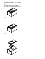
Page 64: ...012 SPEAKER DISASSEMBLY INSTRUCTIONS Type 4 qllip 1 2 3 E F Fig 1 Fig 2 Fig 3 1 2 3 64 012 Q 012345 m kbiI co NK m kbiI co m kbiI pmho 0cáÖJN OK 0 cáÖJO m kbiI co PK cáÖJP m kbiI co m kbiI co m kbiI pmho m kbiI co m kbiI co ...

Page 65: ...DISASSEMBLY INSTRUCTIONS Insert a flat bladed screwdriver into the position indicated by the arrows and remove the panel Remove the screws of each speaker unit and then remove the speaker units Type 1 Type 3 Type 2 ...

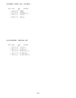
Page 66: ...0 010 SPKR W 130 6 8A CJ4 501 010 CORD SP 7 8A CJ5 417 010 SPKR TW 25 ACCESSORIES PACKAGE LIST DESCRIPTION REF NO KANRI NO PART NO 1 8A CJ4 905 010 IB K E I K 1 8A CJ4 906 010 IB EZ 9L I EZ 1 8A CJ4 908 010 IB D J I D 2 87 006 225 010 1D AM LOOP ANT NC2 3 87 A90 118 010 ANT WIRE FM Z K EZ 3 87 043 115 010 1A ANT FEEDER FM D 4 8A CJ4 951 010 RC UNIT RC AAT04 D 4 8A CJ4 952 010 RC UNIT RC AAT05 K EZ...

Page 67: ...2 11 IKENOHATA 1 CHOME TAITO KU TOKYO 110 JAPAN TEL 03 3827 3111 Printed in Singapore 9301978 0251431 ...

Page 68: ... D K EZ S M Code No 09 004 422 8S1 SUPPLEMENT This Service Manual contains the additional information DISASSEMBLY INSTRUCTION and TEST MODE for the model XR MD510 511 K EZ If requiring the other information see Service Manual of XR MD510 D K 511 EZ S M Code No 09 004 422 8R1 MODEL CODE 8ACJ4 0130 S 8ACJ4 0133 SM XR MD510 511 SYSTEM SPEAKER SX M510 ...

Page 69: ...2 1 外観部品をはずす 1 ビス6本 1 4 2 2 をはずし PANEL SIDE Rをはずす 2 ビス6本 1 4 2 2 をはずし PANEL SIDE Lをはずす 3 ビス3本1をはずし PANEL TOP ASSY2を持ち上げる 4 コネクターを2箇所はずし PANEL TOP ASSYをはずす DISASSEMBLY INSTRUCTION R L ...

Page 70: ...3 5 ビス11本をはずし CABI REARをはずす 6 外観部品がはずれた状態 2 PWB CD ACJ 4 をはずす 1 ビス5本はずし FFC 等を抜き PWB CD ACJ 4をはずす 3 PWB MAIN ASSY をはずす 1 ビス1本1はずし コネクタ2とMD部のFFC3をはずす ...

Page 71: ...ビス1本1はずし PWB MAIN ASSYを矢印方向2にはずす 基板がフックされているので HOOKを持ち上 げながら基板をはずす 4 FRONT 部をはずす 1 CAB FR ASSYを止めているビス1と CHAS MDを止めているビス2をはずす 2 CAB FR ASSYを止めているビス1と CHAS MDを止めているビス2をはずす 3 ビス2本1をはずし CABI FR ASSYを矢印2方向にはずす ...

Page 72: ...5 4 PWB MAIN ASSYとCABI FRONT ASSYがはずれた状態 6 CD 部 3ZG 3 をはずす 1 ビス4本1をはずし CD 部2をはずす 5 MD 部 AZG 4 をはずす 1 ビス4 本をはずし MD 部をはずす 2 CD 部がはずれた状態 ...

Page 73: ...6 延長用FFCを使用する事で CD MDメカニズムを通電 下図参照 修理等が行えます 1FFC 8P 1 25 88 908 401 110 2FFC 8P 1 0 SV J00 043 010 3FFC 14P 1 0 SV J00 044 010 SERVICE JIG AND TOOLS ...

Page 74: ...e six screws 1 4 2 2 and remove the PANEL SIDE R 2 Remove the six screws 1 4 2 2 and remove the PANEL SIDE L 3 Remove the three screw 1 and lift up the PANEL TOP ASSY 2 4 Remove the two connectors and remove the PANEL TOP ASSY R L DISASSEMBLY INSTRUCTION ...
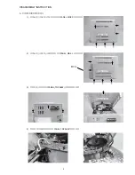
Page 75: ... after the outside appearance parts are removed 2 Removing the PWB CD ACJ 4 1 Remove the five screws pull out the FFC and other parts then remove the PWB CD ACJ 4 3 Removing the PWB MAIN ASSY 1 Remove the screw 1 then remove the connector 2 and the FFC 3 of the MD block ...

Page 76: ... up the HOOK remove the board 4 Removing the FRONT block 1 Remove the screw 1 securing the CAB FR ASSY and remove the screw 2 securing the CHAS MD 2 Remove the screw 1 securing the CAB FR ASSY and remove the screw 2 securing the CHAS MD 3 Remove the two screws 1 and remove the CABI FR ASSY in the direction of arrow 2 ...

Page 77: ...SY and CABI FRONT ASSY are removed 5 Removing the MD block AZG 4 1 Remove the four screws and remove the MD block 6 Removing the CD block 3ZG 3 1 Remove the four screws 1 and remove the CD block 2 2 This is the state after the CD block is removed ...

Page 78: ... extension enables the CD MD mechanism to be repaired when the power supply is turned on Refer to the below figure 1 FFC 8P 1 25 88 908 401 110 2 FFC 8P 1 0 SV J00 043 010 3 FFC 14P 1 0 SV J00 044 010 SERVICE JIG AND TOOLS ...

Page 79: ...12 組み立て時の注意 マジカルチェンジパネルを組み込むときにギアの位相あわせを行ってください 1 GEAR OPE 1 とGEAR WORM WHEEL の位相あわせ 1 1の穴をあわせる 2 同時に各 GEAR の穴の位置を図中2のようにする 2 HLDR GEAR ASSY の組み込み方法 1 図の PANEL 面が正面に来るようにする 2 HLDR GEAR ASSY を組み込む ...

Page 80: ...ase adjustment of the GEAR OPE 1 and GEAR WORM WHEEL 1 Align holes 1 2 Then move the position of the holes of each gear as shown by 2 in the illustration 2 Installation Procedure of HLDR GEAR ASSY 1 Position the panel side so that it faces front as shown in the illustration 2 Install the HLDR GEAR ASSY ...

Page 81: ...タートして下さい モード スタートモード フォーカス サーチモード プレイモード トラバースモード スレッドモード 操作方法 CD キー AC プラグ IN STOP キー PLAY キー PAUSE キー F SKIP キー B SKIP キー ディスプレイ表示 全灯表示 CD トラック No 経過時間 スペアナ トラック No 経過時間 CD TEST 機能 動作 CD TEST MODE スタート ディスプレイ全灯 LD 発光 連続フォーカスサーチ 連続スピンドルモータ キック 通常再生 TOC READ 出来ない場合 フォーカスサーチ続行 トラッキングサーボ OFF ピックアップ内周へ移動 ピックアップ外周へ移動 確認項目 ディスプレイ点灯確認 マイコン DATA BUS LINE APC 回路 LASER 電流 フォーカスサーチ波形確認 フォーカスエラー波形確認 フォーカスサーボ...

Page 82: ... mode Sled mode Operation CD key AC plug IN STOP key PLAY key PAUSE key F SKIP key B SKIP key Indication on display All indicators light CD Track No and playing time spectrum analyzer Track No and playing time CD TEST Function and movement CD TEST mode starts All indicators light LD lights Continuous focus search Continuous spindle motor kick Normal playback When TOC reading is not possible the fo...

Page 83: ...操作時の注意点 テストモ ドを起動すると 操作パネルのTOUCH SENSORがきかなくなります 下記の方法で操作してください 1 リモコンを使用する 2 CD基板に設けられた穴から見えるPULLEYを手で回し 操作パネルを回転させる 6 スレッド送り動作の確認 1 ALL SV OFF からF SKIPボタンを押すと レンズとピックアップは外周方向に移動します その時 ディスプレイは T SLED FWD と表示します 2 ALL SV OFF からB SKIPボタンを押すと レンズとピックアップは内周方向に移動します その時 ディスプレイは T SLED RVS と表示し INSIDE LIMIT SWがONするとディスプレイの グラフィックイコライザ JAZZ の枠が点灯します 7 レ ザ パワ の確認 1 ALL SV OFF からMD EDITボタンを押す毎にレ ザ パワ の切り...

Page 84: ...ISCによってサ ボのモ ドを下記の様に合わせます MO DISC ディスプレイ表示 SELECT GRV TIMRMARK 点灯 PIT DISC ディスプレイ表示 SELSCT PIT AUTOMARK 点灯 3 PLAYボタンを押します フォ カスサ ボが正常の場合 ディスプレイは FOCUS SRCH の後 FOCUS ON と 表示します 4 確認後STOP ボタンを押し ALL SV OFF にします 10 4 オ ルサ ボONの確認 1 フォ カスサ ボONの状態からENTERボタンを押すと トラッキング スレッドサ ボがONし すべてのサ ボが 働きます 全サ ボが正常の場合 ディスプレイは ALL SV ON と表示します 2 確認後STOP ボタンを押し ALL SV OFF にします 機能名称 レーザーパワー ディスクタイプ REC PROTECT SW REFLEC...

Page 85: ...ピックアップのレ ザ 出力をレ ザ パワ メ タ で測定し 約0 68mWになる事を確認してください 5 調整後 STOPボタンを押し ディスプレイ表示を ALL SV OFF にします 2 2 記録レーザーパワー調整 1 ALL SV OFF からMD EDITボタンを3回押し ディスプレイ表示を LASER WRITE に切 り替えます 2 PAUSEボタンを1回押して ディスプレイ表示を LASER にします 3 B SKIP F SKIPボタンで LASER 9F に調整し ENTERボタンを押します 4 ピックアップのレ ザ 出力をレ ザ パワ メ タ で測定し 約6 8mWになる事を確認してください 5 調整後 STOP ボタンを押し ディスプレイ表示を ALL SV OFF にします 注意 レ ザ 出力が7 0mWを越えるとPICK UPが破損する場合があります 3 AUTO...

Page 86: ...t 15 40 s 33 15 40 6 確認後 STOPボタンを押しディスプレイ表示を ALL SV OFF にします 4 再生エラ レ ト確認 PIT DISC テストポイント ディスプレイ表示にて確認 テストディスク TGY 1同等品 1 TGY 1をローディングします 2 B SKIPボタンとF SKIPボタンを使って ピックアップをDISCの中間位置まで移動させます 3 MD MODEボタンを押して SELECT PIT と表示させます 4 PLAYボタンを押して FOCUS ON と表示させます 5 ENTERボタンを押して ALL SV ON と表示させます 6 DISPLAYボタンを1回押してアドレス表示が安定してカウントすることを確認します 7 再度DISPLAYボタンを押すと 再生エラ レ トの表示になります その時の Er 下線部 の数字が Er0030 以下であるこ...

Page 87: ... RECボタンを押して REC Analog と表示させます 5 PLAYボタンを押して FOCUS ON と表示させます 6 ENTERボタンを押して ALL SV ON と表示させます 7 TAPE REC REC MUTEボタンを押して UTOC ERASE と表示させます 8 UTOCの消去が完了すると 自動的に ALL SV OFF の表示に切り替わります 7 EEP ROMの初期化方法 下記の方法により EEP ROM内の調整値をデフォルト 標準値 にします EEP ROMの初期化を行った場合は 必ず MD 電気調整の1 3を行ってください 1 CD OPEN CLOSEボタンを押しながら 本体のMD EDITボタンを押します 2 電源を入れ直した時に NO Adjust と表示される事を確認してください NO Adjust の状態でも MD 動作させることができます ...

Page 88: ...F 5 Notes during Test Mode Operation If the test mode starts up the touch sensor of the operation panel does not run Operate in the following ways 1 Use the remote controller 2 Rotate the pulley that is visible from the hole of the CD board by hand to rotate the operation panel 6 Checking the Sled Feed Operation 1 Press the F SKIP button in the ALL SV OFF state to move the lens and pickup to the o...

Page 89: ...k 2 Press the MD MODE button and set the servo mode according to the inserted disk as shown below MO disk SELECT GRV appears and TIMEMARK lights PIT disk SELECT PIT appears and AUTOMARK lights 3 Press the PLAY button If the focus servo is normal FOCUS SRCH appears and FOCUS ON appears 4 After checking press the STOP button to return the display to ALL SV OFF 10 4 Checking the All Servo ON 1 When t...

Page 90: ... to LASER 11 using the B SKIP and F SKIP buttons and press the ENTER button 4 Measure the pickup laser output using the laser power meter and adjust it using the B SKIP button and F SKIP button so that it is around 0 68 mW 5 After adjustment press the STOP button to change the display to ALL SV OFF 2 2 Recording Laser Power Adjustment 1 Press the MD EDIT button three times in the ALL SV OFF state ...

Page 91: ... disk Test point Check the test point on the display Test disk TSYS 1 or equivalent 1 Load the TGYS 1 2 Move the pickup to the center of the disk using the B SKIP button and F SKIP button 3 Press the MD MODE button to display SELECT PIT 4 Press the PLAY button to display FOCUS ON 5 Press the ENTER button to display ALL SV ON 6 Press the DISPLAY button once to confirm that the address indication is...

Page 92: ...lay REC Analog 5 Press the PLAY button to display FOCUS ON 6 Press the ENTER button to display ALL SV ON 7 Press the TAPE REC REC MUTE button to display UTOC ERASE 8 After deleting the UTOC the display automatically returns to ALL SV OFF 7 Initializing Procedure of EEP ROM Follow the procedure given below to set the adjustment value of EEP ROM to the default value reference value 1 While pressing ...

Page 93: ...2 11 IKENOHATA 1 CHOME TAITO KU TOKYO 110 JAPAN TEL 03 3827 3111 Printed in Singapore 9301978 0251431 ...

Reviews: