background image

– 30 –

< DECK  SECTION >

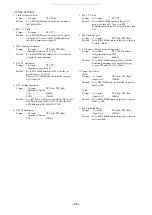
12. Tape Speed Adjustment (DECK 2)

Settings : • Test tape : TTA–100

• Test point : TP5(Lch), TP6(Rch)
• Adjustment location : SFR1

Method : Play back the test tape and adjust SFR1 so that the

frequency counter reads 3000Hz 

±

 5Hz and 

±

45Hz

(REV) with respect to forward speed.

13. Head Azimuth Adjustment (DECK 1, DECK 2)

Settings : • Test tape : TTA–330

• Test point : TP5(Lch), TP6(Rch)
• Adjustment location : Head azimuth

adjustment screw

Method : Play back (FWD) the 8kHz signal of the test tape and

adjust screw so that the output becomes maximum.
Next, perform on REV PLAY mode.

14. PB Frequency Response Check (DECK 1, DECK 2)

Settings : • Test tape : TTA–330

• Test point :TP5(Lch), TP6(Rch)

Method : Play back the 315Hz and 8kHz signals of the test tape

and check that the output ratio of the 8kHz signal with
respect to that of the 315Hz signal is within 5dB.

15. PB Sensitivity Check (DECK 1, DECK 2)

Settings : • Test tape : TTA–200

• Test point : TP5(Lch), TP6(Rch)

Method : Play back the test tape and check that the output level of

the test point is 140mV 

±

 3dB.

16. REC/PB Frequency Response Adjustment (DECK 2)

Settings : • Test tape : TTA–602

• Test point : TP5(Lch), TP6(Rch)
• Input signal : 1kHz / 8kHz (LINE IN)
• Adjustment location : SFR451 (Lch)

SFR452 (Rch)

Method : Apply a 1kHz signal and REC mode. Then adjust

OSC attenuator so that the output level at the TP5,
TP6 becomes -20VU. Record and play back the 1kHz
and 8kHz signals and adjust SFRs so that the output of
the 8kHz signals becomes 0.5dB 

±

 0.5dB with respect to

that of the 1kHz signal.

17. REC/PB Sensitivity Check (DECK 2)

Settings : • Test tape : TTA–602

• Test point : TP5(Lch), TP6(Rch)
• Input signal : 1kHz (LINE IN)

Method : Apply a 1kHz signal and REC mode. Then adjust

OSC attenuator so that the output level at TP5, TP6
becomes 0VU. Record and play back the 1kHz signals
and check that the output is 0dB 

±

 3.0dB.

< MICON  SECTION >

18.

µ

-CON OSC Adjustment

Settings : • Test point : TP7 (O-KSCAN)

• Adjustment location : L101

Method : Insert AC plug while pressing TUNER function key.

Adjust L101 so that the frequency at the test point is
208.80Hz 

±

 0.21Hz.

All manuals and user guides at all-guides.com

Summary of Contents for Z-L500

Page 1: ...Manual Z L500 K EZ S M Code No 09 002 424 0T2 If requiring information about the CD mechanism see Service Manual of 6ZG 1 S M Code No 09 001 338 7N2 If requiring information about the Stereo Turntable see Service Manual of PX E860 K S M Code No 09 993 322 0R4 Z L500 EZ SPEAKER SYSTEM CD CASSEIVER SX WZL500 CX ZL500 REMOTE CONTROLLER Z L500 K RC ZAS02 PX E860 STEREO TURNTABLE All manuals and user g...

Page 2: ... or more PHONES stereo jack accepts headphones of 32 ohms or more Cassette deck section Track format 4 tracks 2 channels stereo Frequency response 50 Hz 12500 Hz Recording system AC bias Heads Deck 1 Playback head x 1 Deck 2 Recording Playback head x 1 erase head x 1 Compact disc player section Laser Semiconductor laser λ 780 nm D A converter 1 bit dual Signal to noise ratio 85 dB 1 kHz 0 dB Harmo...

Page 3: ...ätt än vad som specificeras i denna bruksanvising kan användaren utsättas för osynling laserstrålning som överskrider gränsen för laserklass 1 PROTECTION OF EYES FROM LASER BEAM DURING SERVICING CAUTION Use of controls or adjustments or performance of proce dures other than those specified herin may result in hazardous radiation exposure ATTENTION L utillisation de commandes réglages ou procédures...

Page 4: ...irm that the main power is turned on and the HOLD terminal of the MICROCOMPUTER keeps the H level or not 3 3 3 3 3 When the HOLD terminal is L level the abnormality detection circuit is judged to be working correctly and the MICROCOMPUTER is judged to be good 1 Forced discharge of electrolytic capacitor of power supply block When repair is going to be attempted in the set that uses relay circuit i...

Page 5: ...ic capacitor C113 that is connected to VDD of the MICROCOMPUTER with tweezers 3 3 3 3 3 Connect the AC power cord again If the MICROCOMPUTER returns to the normal operation the MICROCOMPUTER is good Note The reference number or MICROCOMPUTER pin number of transistor Q110 and electrolytic capacitor C113 can change depending on the models Be sure to check the reference numbers on schematic diagram b...

Page 6: ...P E 3300 50 C21 87 A10 520 000 CAP E 3300 35 SME C22 87 A10 520 000 CAP E 3300 35 SME C23 87 A10 520 000 CAP E 3300 35 M SME C24 87 A10 520 000 CAP E 3300 35 M SME C25 87 010 247 080 CAP ELECT 100 50V C26 87 010 247 080 CAP ELECT 100 50V C30 87 010 430 080 CAP ELECT 100 63V C31 87 010 263 080 CAP ELECT 100 10V C32 87 010 197 080 CAP CHIP 0 01 25 KB C2012 C34 87 010 247 080 CAP ELECT 100 50V C35 87...

Page 7: ...AP ELECT 220 25V C618 87 010 405 080 CAP ELECT 10 50V C620 87 010 263 080 CAP ELECT 100 10 M 11L SME C630 87 A10 201 080 CAP S 0 33 16 C631 87 010 185 080 C CAP S 3900P 50 B C632 87 010 185 080 C CAP S 3900P 50 B C633 87 010 193 080 CHIP CAPACITOR 0 033 25 C634 87 010 193 080 CHIP CAPACITOR 0 033 25 C669 87 010 322 080 C CAP S 100P 50 CH C670 87 010 322 080 C CAP S 100P 50 CH C673 87 010 182 080 C...

Page 8: ...00P 50 J CH GRM R995 87 010 322 080 C CAP S 100P 50 J CH GRM SFR451 87 A90 432 080 SFR 30K H NVZ6TLTA SFR452 87 A90 432 080 SFR 30K H NVZ6TLTA TC942 87 011 253 080 TRIMMER CER 30P 4 0X4 5 WH1 87 A91 179 010 HLDR WIRE 2 5 11P X861 87 A70 091 010 VIB XTAL 4 332MHZ CSA 309 X991 87 A70 061 010 VIB XTAL 4 500MHZ CSA 309 MICON C B C101 87 010 498 040 CAP E 10 16 M 5L SRE C102 87 010 194 080 CAP CHIP 0 0...

Page 9: ...11G04M S826 87 A90 095 080 SW TACT EVQ11G04M S827 87 A90 095 080 SW TACT EVQ11G04M S828 87 A90 095 080 SW TACT EVQ11G04M S829 87 A90 095 080 SW TACT EVQ11G04M S830 87 A90 095 080 SW TACT EVQ11G04M S831 87 A90 095 080 SW TACT EVQ11G04M S836 87 A90 095 080 SW TACT EVQ11G04M S837 87 A90 095 080 SW TACT EVQ11G04M S838 87 A90 095 080 SW TACT EVQ11G04M S842 87 A90 095 080 SW TACT EVQ11G04M S843 87 A90 0...

Page 10: ... A CHIP RESISTOR PART CODE 0 55 Resistor Code Dimensions mm Symbol 1 16W 1005 5 CJ 1 0 0 5 0 35 104 L t W E C B KTA1266GR KTC3198GR CD1585BC CSA952K E C B 2SC3331 T U 2SB1370 DTC114ES KTC3199GR CSC4115BC E C B B C E E B C 2SA1235F 2SC2714O 2SC3052F CMBT5551 CMBT5401 RT1N144C 2SD1306E KRA102S KRC102S RTK KRA107S CSD1306E RT1P141C S G D 2SK2158 2SJ461 T1 E C B 2SJ460 2SK2541 S D G G D S 2SK360E All ...

Page 11: ...1 MAIN 11 10 11 12 13 14 15 16 17 18 19 20 21 22 23 24 A B C D E F G H I J K L M N O P Q R S T U 1 2 3 4 5 6 7 8 9 25 26 27 28 29 30 31 32 All manuals and user guides at all guides com a l l g u i d e s c o m ...

Page 12: ...SCHEMATIC DIAGRAM 1 MAIN 1 2 AMP SECTION 12 All manuals and user guides at all guides com ...

Page 13: ...SCHEMATIC DIAGRAM 2 MAIN 2 2 TUNER SECTION 13 All manuals and user guides at all guides com ...

Page 14: ...WIRING 2 MICON 14 10 11 12 13 14 15 16 17 18 19 20 21 22 23 24 A B C D E F G H I J K L M N O P Q R S T U 1 2 3 4 5 6 7 8 9 25 26 27 28 29 30 31 32 All manuals and user guides at all guides com ...

Page 15: ...SCHEMATIC DIAGRAM 3 MICON DECK 15 All manuals and user guides at all guides com ...

Page 16: ...NTL KEY CD 16 10 11 12 13 14 15 16 17 18 19 20 21 22 23 24 A B C D E F G H I J K L M N O P Q R S T U 1 2 3 4 5 6 7 8 9 25 26 27 28 29 30 31 32 All manuals and user guides at all guides com a l l g u i d e s c o m ...

Page 17: ...SCHEMATIC DIAGRAM 4 CNTL KEY CD 17 All manuals and user guides at all guides com ...

Page 18: ...WIRING 4 PT 18 CNA001 10 11 12 13 14 15 16 17 18 19 20 21 22 23 24 A B C D E F G H I J K L M N O P Q R S T U 1 2 3 4 5 6 7 8 9 25 26 27 28 29 30 31 32 All manuals and user guides at all guides com ...

Page 19: ...SCHEMATIC DIAGRAM 5 PT 19 All manuals and user guides at all guides com ...

Page 20: ...5 7 9 11 FC104 F DECK C B FROM B MICON C B CN104 10 11 12 13 14 15 16 17 18 19 20 21 22 23 24 A B C D E F G H I J K L M N O P Q R S T U 1 2 3 4 5 6 7 8 9 25 26 27 28 29 30 31 32 All manuals and user guides at all guides com ...

Page 21: ...rol 26 RDS_SG I During TUNER FUNC RDS Signal level input 27 TM BASE I Reference signal input for clock 28 I SENS I During CD FUNC CD DSP SENS input RDS CK During TUNER FUNC RDS serial clock input 29 REM I Remote control signal input 30 42 G13 G1 O FL grid G13 G1 output 43 45 P38 P36 O FL segment P38 P36 output 46 VDD Power supply 47 P35 SPEANA A O FL segment P35 output Spectrum analyser BPF switch...

Page 22: ...segment P13 output Deck 2 cassette existence detection SW input L Existent 71 P12 REA O I FL segment P12 output Deck 2 side A recording able disable detection SW input L Able 72 VDD Power supply 73 83 P11 P1 O FL segment P11 P1 output 84 P39 PB1 O I FL segment P39 output Deck 1 2 select control H Deck 1 85 KEYSCAN O Segment input timing output L Input timing 86 MOTOR O DECK MECHA motor control out...

Page 23: ... 23 IC BLOCK DIAGRAM IC BU2099FV IC LC72131D All manuals and user guides at all guides com ...

Page 24: ... 24 IC M61506FP IC LA1843 All manuals and user guides at all guides com ...

Page 25: ... 25 IC M61503FP IC BU1920FS All manuals and user guides at all guides com ...

Page 26: ... 26 FL BJ746GNK GRID ASSIGNMENT ANODE CONNECTION GRIDASSIGNMENT All manuals and user guides at all guides com a l l g u i d e s c o m ...

Page 27: ... 27 ANODECONNECTION All manuals and user guides at all guides com ...

Page 28: ...5 LCH TP6 RCH 12 2 L802 9 3 TP1 VT 3 3 1 3 FFE831 O KSCAN 18 MICON C B B FL101 L101 SFR1 12 TP3 DC BALANCE 6 1 4 5 6 8 10 11 13 14 15 9 16 18 IC801 3 IC101 TP7 TP8 GND 13 DECK C B F DECK 1 P HEAD DECK 2 R P E HEAD FWD 13 REV 16 17 7 L941 L942 TC943 5 4 All manuals and user guides at all guides com ...

Page 29: ... adjusted to MAX by TC943 6 AM IF Adjustment Settings Test point TP5 Lch TP6 Rch Adjustment location L802 450kHz 7 FM VT Check Settings Test point TP1 VT Method Set to FM 108 0MHz and check that the test point is less than 8 0V Then set to FM 87 5MHz and check that the test point is more than 0 5V 8 FM Tracking Check Settings Test point TP5 Lch TP6 Rch Method Set to FM 98 0MHz and check that the t...

Page 30: ...ay back the test tape and check that the output level of the test point is 140mV 3dB 16 REC PB Frequency Response Adjustment DECK 2 Settings Test tape TTA 602 Test point TP5 Lch TP6 Rch Input signal 1kHz 8kHz LINE IN Adjustment location SFR451 Lch SFR452 Rch Method Apply a 1kHz signal and REC mode Then adjust OSC attenuator so that the output level at the TP5 TP6 becomes 20VU Record and play back ...

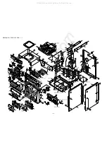
Page 31: ... 31 MECHANICAL EXPLODED VIEW 1 1 All manuals and user guides at all guides com a l l g u i d e s c o m ...

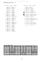
Page 32: ...10 HLDR LOCK 1 22 87 B00 002 010 BADGE AIWA 30 ABS SIL 23 8A MA3 093 010 KNOB ASSY RTRY JOG 24 8A MA5 031 010 PANEL FR RDS 5 25 8A MA5 080 010 KEY ASSY GEQ 5M 26 8A MA3 084 010 KEY ASSY FF 27 8A MA5 066 010 KEY FUN 4F 28 8A MA5 081 010 KEY ASSY PLAY 29 8A MA3 071 010 KEY TIMER 30 8A MA3 073 010 KEY ENTER 31 8A MA3 210 010 GUIDE LED OPE 32 8A MA3 057 010 WINDOW TOP 33 8A MA3 020 110 CABI TOP 34 8A ...

Page 33: ...3 14 14 15 15 16 16 17 18 18 19 19 20 20 21 21 30 22 23 24 25 26 27 28 22 23 24 25 26 27 28 29 31 32 33 34 35 36 37 37 38 38 39 39 40 41 42 43 44 51 52 45 46 47 48 49 50 53 54 54 56 55 30 35 29 31 32 33 52 51 44 45 43 42 IC EW732 IC EW732 b a a b c c 40 41 46 47 48 49 P C B All manuals and user guides at all guides com ...

Page 34: ...010 GEAR SLIP F R A M3 27 8Z ZM1 269 010 FELT FF REW 2 28 8Z ZM1 238 110 GEAR SLIP FF REW B 2 29 8Z ZM3 220 010 LEVER FR M3 30 8Z ZM3 205 010 LEVER PLAY M3 31 8Z ZM3 233 010 SPR T BRG M3 32 84 ZM2 227 310 SPR C AZIMUTH 33 87 A90 403 110 HEAD RPH MS15R 34 87 A90 404 010 HEAD EH LE15B 35 8Z ZM3 239 010 SPR E FR 36 8Z ZM3 211 010 LEVER EJECT R 37 8Z ZM3 225 010 LEVER STOP 38 8Z ZM3 221 010 LEVER CAS ...

Page 35: ...ction until click sound comes out Remove the grill frame and four pieces of rubber caps by pulling out with a flat bladed screwdriver Remove the screws from hole where installed rubber caps Insert a flat bladed screwdriver into the position indicated by the arrows and remove the panel Re move the screws of each speaker unit and then remove the speaker units TOOLS 1 Plastic head hammer 2 flat head ...

Page 36: ...5 604 010 SPKR M 120 7 88 MS1 608 010 SPKR CERAMIC 8 88 NS3 605 010 CAP 9 88 MS1 610 010 CORD SPKR 10 88 NS5 611 010 CORD SPKR B L 11 8A MS5 013 010 CORD PACKING DESCRIPTION REF NO KANRI NO PART NO ACCESSORIES PACKAGE LIST 1 8A MA5 905 010 IB K E M K 1 8A MA5 906 010 IB EZ 9L M EZ 2 8Z NF9 701 210 RC UNIT ZAS02 3 87 A90 118 010 ANT WIRE FM Z 4 87 A90 030 010 ANT LOOP AM NC C All manuals and user g...

Page 37: ...2 11 IKENOHATA 1 CHOME TAITO KU TOKYO 110 JAPAN TEL 03 3827 3111 Printed in Singapore 9420208 9630472 0251431 All manuals and user guides at all guides com ...
Reviews: