background image

-18-

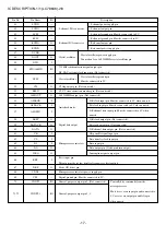
Pin No.

Pin Name

I/O

Description

IC DESCRIPTION-1/1 (LC78646)-3/3

73, 74

75

76

77

78

79

80

PD01, 2

VVSS

PCKIST

VVDD

FR

LDS

LDD

O

I

I

I

O

Phase comparison output pin 1, 2 to control built-in VCO.

Built -in VCO GND pin. Must always be connected to 0V.

PLL

Resistor connection pin to set current for PD01 and 02 outputs.

Built-in VCO power supply pin.

Resistor connection pin to set the frequency range of built-in VCO.

Laser power detection signal input pin.

Laser power control signal output pin.

Summary of Contents for ZD5GNDM

Page 1: ...SERVICE MANUAL D A T A BZG 5 English CD MECHANISM TYPE ZD5GNM ZD5GNDM BASIC CD MECHANISM KSM 213 RSCM KSM 213 RSCM S M Code No 09 023 353 3NC BASIC CD MECHANISM KSM 213 RSCM ...

Page 2: ...han those specified herein may result in hazardous radiation exposure ATTENTION L utilisation de commandes réglages ou procédures autres que ceux spécifiés peut entraîner une dangereuse exposition aux radiations ADVARSEL Usynlig laserståling ved åbning når sikkerhedsafbrydereer ude af funktion Undgå udsættelse for stråling This Compact Disc player is classified as a CLASS 1 LASER product The CLASS...

Page 3: ...213R 1 After the connection remove solder shown in the right figure Body or clothes electrostatic potential could ruin laser diode in the optical block Be sure ground body and workbench and use care the clothes do not touch the diode Solder PICK UP Assy PWB ...

Page 4: ...MECHA as shown below 3 Confirm that the Slide Mech Cam is located in the right position then insert the TRAY gently Caution If the rotating phase of the Gear Main Cam is incorrectly adjusted the chucking operation and tray movement will have malfunction Align the arrow mark with the black round mark How to Adjust the Rotating Phase of the Gear Main Cam ...

Page 5: ... F CM CB a b 3CD O C 0131 87 010 759 080 C CAP U 0 1 25 Z F CM CB a b 3CD O C 0132 87 A12 062 080 CAP E 100 10 SMG a b 3CD O C 0133 87 A10 918 080 CAP E 100 16 SMG a b 3CD O C 0134 87 010 759 080 C CAP U 0 1 25 Z F CM CB a b 3CD O C 0135 87 A12 071 080 CAP E 47 25 SMG a b 3CD O C 0136 87 010 759 080 C CAP U 0 1 25 Z F CM CB a b 3CD X C 0137 88 108 000 080 C JUMPER U a b 3CD O C 0138 87 012 349 080...

Page 6: ...b 3CD X R 0128 88 100 000 010 PLATING JW 0 58 SN95 a b 3CD X R 0129 88 100 000 010 PLATING JW 0 58 SN95 a b 3CD X R 0130 88 121 103 080 RES 10K 1 8W J a b 3CD X R 0131 88 128 473 080 C RES 47K 1 8W J a b 3CD O R 0134 88 108 102 080 C RES U 1K 1 16W J a b 3CD O R 0135 88 108 102 080 C RES U 1K 1 16W J a b 3CD O R 0151 88 108 101 080 C RES U 100 1 16W J a b 3CD O R 0152 88 108 101 080 C RES U 100 1 ...

Page 7: ...t the spare parts centers Components marked X and R are not designated as spare parts for after sales service and will not be stocked at the spare parts centers UNIT NAME C REF NO PARTS NO PARTS NAME SUFFIX MODEL 7 ELECTRICAL PARTS LIST 3 4 T T C B 1 1 CZA 1 CZA 1 ZD5NDM ZD5NM TT O C 0401 87 A11 148 080 CAP TC U 0 1 50 Z F a b TT O CN 0401 86 NFZ 675 010 CONN 5P H 6216 11H a b TT O PS 0401 87 A90 ...

Page 8: ...pon the order is received ELECTRICAL PARTS LIST 4 4 8 8 A Resistor Code Chip Resistor Part Coding Figure Value of resistor Chip resistor Wattage Type Tolerance 1 16W 1 10W 1 8W 1608 2125 3216 5 5 5 CJ CJ CJ Form L W t 1 6 0 8 0 45 2 1 25 0 45 3 2 1 6 108 118 128 A A CHIP RESISTOR PART CODE 0 55 Resistor Code Dimensions mm Symbol 1 16W 1005 5 CJ 1 0 0 5 0 35 104 L t W ...

Page 9: ... 9 TRANSISTOR ILLUSTRATION 1 1 2SA1235F B E C E C B 2SC5343Y 2SA1980G ...

Page 10: ... 10 BLOCK DIAGRAM 1 1 ...

Page 11: ... 11 10 11 12 13 14 15 16 17 18 19 20 21 22 23 24 A B C D E F G H I J K L M N O P Q R S T U 1 2 3 4 5 6 7 8 9 25 26 27 28 29 30 31 32 WIRING 1 2 3CD 1 7 8 2 1 5 1 16 1 6 6 2 5 1 ...

Page 12: ... 12 SCHEMATIC DIAGRAM 1 1 3 ...

Page 13: ... 13 1 2 3 4 5 6 7 8 9 10 11 12 13 14 15 A B C D E F G H I J K L M N O P Q R S T U WIRING 2 2 T T CN202 ...

Page 14: ...DIV 1V Pin 0 Level TIME DIV 200mS IC101 Pin FE VOLT DIV 500mV TIME DIV 5mS IC101 Pin TE VOLT DIV 200mV TIME DIV 200µS 1 45Vp p 1 24Vp p IC101 Pin RES IC101 Pin VDD5 IC101 Pin XOUT 6Vp p 5 2Vp p 1 2Vp p VOLT DIV 1V TIME DIV 10mS VOLT DIV 500mV TIME DIV 200mS 1 6Vp p 1 6Vp p 0 ...

Page 15: ... 15 IC BLOCK DIAGRAM 1 1 IC LA6568 ...

Page 16: ...nected to 0V Tracking control output pin D A output Focus control output pin D A output Spindle control output pin D A output Thread control output pin D A output Servo D A general purpose output pin Not connected General purpose input output pin 4 5 Controlled by commands from the microprocessor General purpose input output pin 6 Any of these that are unused must be either set up as or subcode re...

Page 17: ...round pin Must be connected to 0V C2 flag output pin Not connected C1 C2 error correction monitor pin Not connected 16 9344MHz output pin Not connected L R clock input pin Must be connected to 0V when unused Antishock mode Bit clock input pin Must be connected to 0V when unused L R channel data input pin Must be connected to 0V when unused L R clock output pin Not connected Digital data output Bit...

Page 18: ... comparison output pin 1 2 to control built in VCO Built in VCO GND pin Must always be connected to 0V PLL Resistor connection pin to set current for PD01 and 02 outputs Built in VCO power supply pin Resistor connection pin to set the frequency range of built in VCO Laser power detection signal input pin Laser power control signal output pin ...

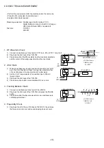
Page 19: ...orm Check connect the output terminal of an oscilloscope to the input terminal of a jitter meter 2 Set the VOLT range selector of an oscilloscope to 500 mV range or lower 3 Play back the 2nd track of the TCD 782 4 Check to see that a jitter meter indicates 40 0 ns or less 3 Tracking Balance Check 1 Connect an oscilloscope to test point TE VREF 2 Play back the 2nd track of the TCD 782 and press the...

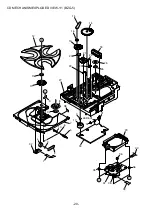
Page 20: ... 20 CD MECHANISM EXPLODED VIEW 1 1 BZG 5 A B 2 3 4 37 5 10 7 8 9 13 11 12 29 27 17 3 26 22 23 21 20 19 16 14 15 24 18 25 1 6 39 38 30 36 36 35 35 33 34 28 C C LED 601 31 32 ...

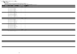
Page 21: ...269 010 GEAR MAIN TT 4 a b O SC1014 84 ZG1 209 010 BELT SQ1 8 117 7 a b O SC1015 84 ZG1 203 410 GEAR MAIN CAM a b O SC1016 84 ZG1 207 010 PULLEY RELAY a b O SC1017 87 045 305 010 MOT RF 500TB a b O SC1018 84 ZG1 204 310 SLIDER MECHA CAM a b O SC1019 84 ZG1 274 010 GEAR RELAY 8 a b O SC1020 81 ZG1 291 110 GEAR TRAY RELAY NO3 a b BZG 5 BZG 5 ZD5GNDM ZD5GNM O SC1021 84 ZG1 205 210 GEAR TRAY a b O SC1...

Page 22: ... S Silver ST Titan Silver T Brown V Violet W White WT Transparent White Y Yellow YT Transparent Yellow LM Metallic Blue LL Light Blue GT Transparent Green LD Dark Blue DT Transparent Orange GM Metallic Green YM Metallic Yellow DM Metallic Orange PT Transparent Pink LA Aqua Blue GL Light Green HT Transparent Gray HM Metallic Gray NH Champagne Gold M Wood Pattern COLOR NAME TABLE 1 1 ...

Page 23: ...2 11 IKENOHATA 1 CHOME TAITO KU TOKYO 110 8710 JAPAN TEL 03 3827 3111 0251431 ...

Reviews: