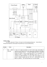

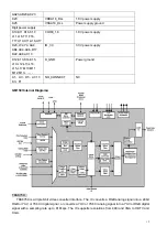


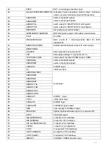
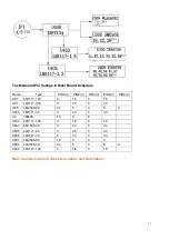

19
4,8,28 NC
No
connection(leave
open or connect to ground)
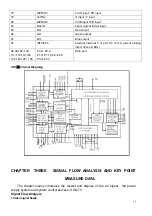
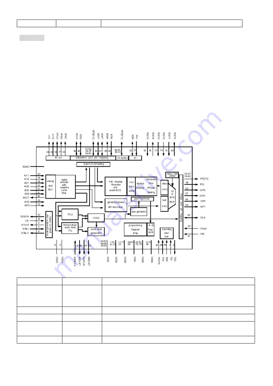
SAA7115
:
The SAA7115 is a video capture device for various applications ranging from small screen products like
e.g. digital set top boxes, personal video recording applications to big screen devices like e.g. LCD
projectors due to it’s improved comb filter performance and 10 bit video output capabilities.
Main Features:
●
Six analog inputs, internal analog source selectors;
●
Two improved 9 Bit CMOS analog-to-digital converter in differential CMOS style;
●
Automatic Clamp Control (ACC) for CVBS, Y and C;
●
Enhanced Horizontal and vertical Sync Detection;
●
PAL delay line for correcting PAL phase errors;
●
Automatic TV/VCR detection;
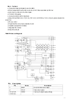
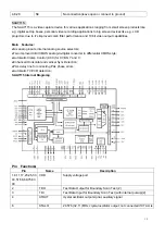
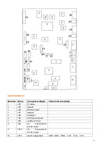
SAA7115 Internal Diagram
:
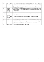
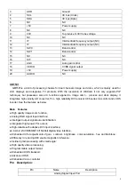
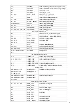
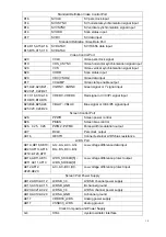
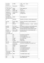
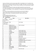
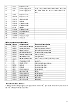
Pin Function
:
Pin Name
Description
1,8,11,17,23,25,33
43,51,58,68,75,83
93
VDD
Supply voltage port
2
TDO
Test Data Output for Boundary Scan Test (2)
3
TDI
Test Data Input for Boundary Scan Test (with internal pull-up)(2)
4
XTOUT
crystal oscillator output signal, auxiliary signal
6
XTALO
24.576 (32.11) MHz crystal oscillator output; not connected if XTALI is