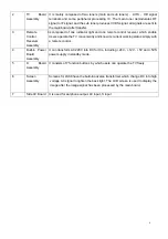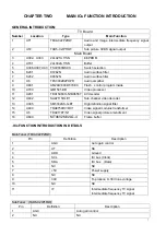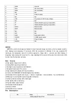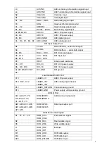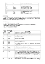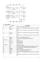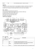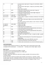
20
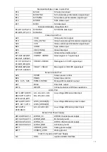
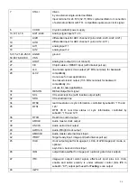
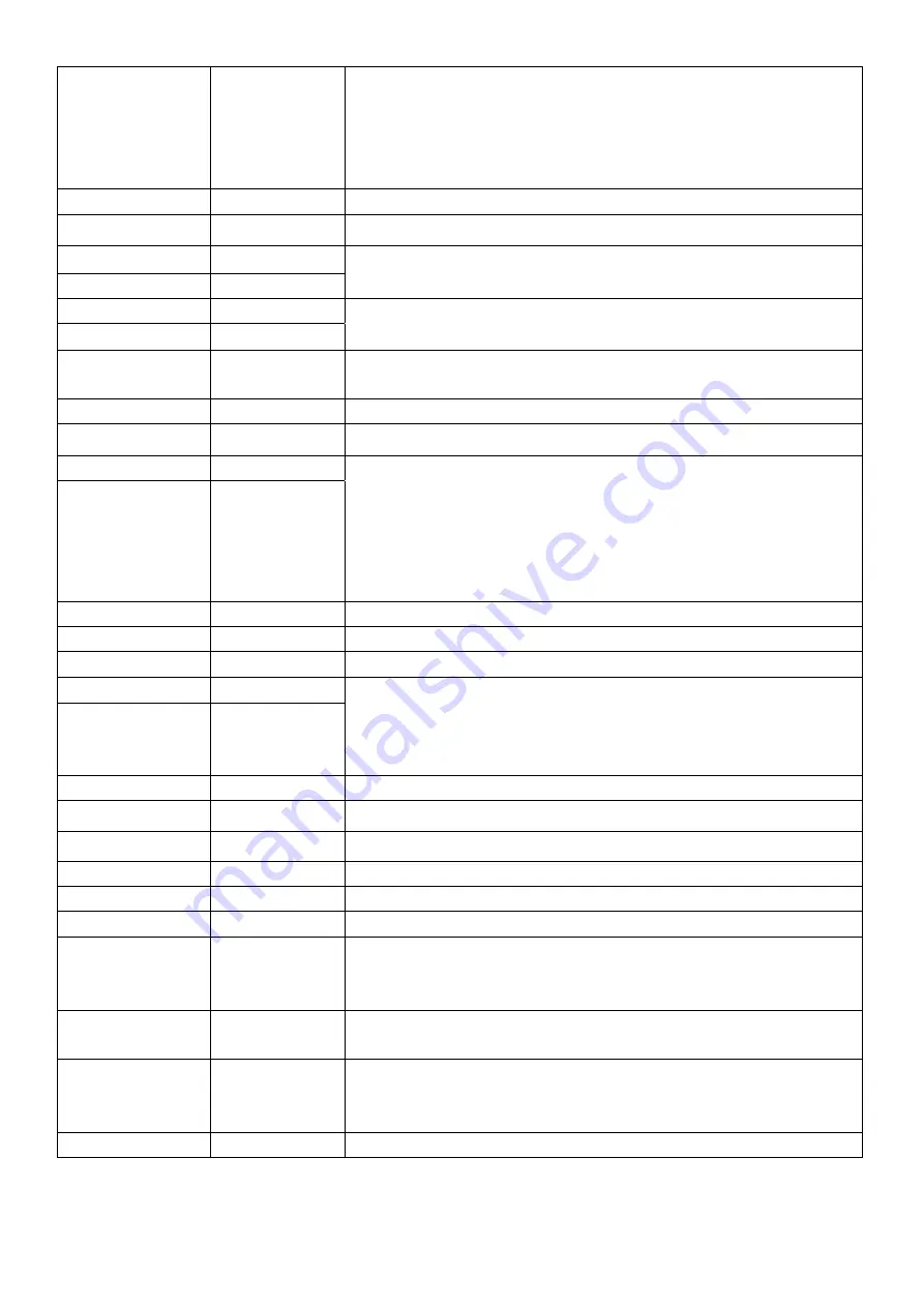
7 XTALI
driven
by an external single-ended oscillator.
Input terminal for 24.576 (32.11) MHz crystal oscillator or connection
of external oscillator with TTL compatible square wave clock signal.
6
VXDD
Crystal oscillator power supply
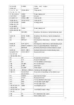
10,12,14,16 AI21~AI24
Analog signal input 21~24
13 AI2D
19 AI1D
differential input for ADC channel 2 (pins AI24, AI23, AI22, AI21)
differential input for ADC channel 1 (pins AI12, AI11)
20 AI11
18 AI12
analog input 11
analog input 12
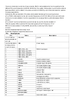
5,9,15,21,24,26,38
50,63,76,88,100
AGND
VSS
ground
22
AOUT
Analog test output (do not connect)
27
CE
Chip Enable or RESET input (with internal pull up)
28 LLC
29 LLC2
line-locked system clock output (27 MHz nominal), for backward
compatibility,
do not use for new applications
line locked clock/2 output (13.5 MHz nominal) for backward
compatibility, do
not use for new applications
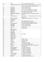
30
RESON
RESet Output Not signal
31
SCL
IIC serial clock line (with inactive output path)
32
SDA
IIC serial data line
34 RTS0
35 RTS1
real time status or sync information, controlled by subaddr. “11h and
12h”
RTS1 35 O real time status or sync information, controlled by
subaddr. “11h and 12h”
36
RTCO
Real time control output
37
AMCLK
Audio master clock output
39
ASCLK
Audio serial clock output
40
ALRCLK
Audio lift/right clock output
41
AMXCLK
Audio master external clock input
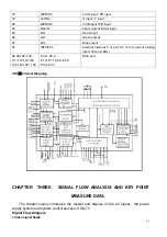
42
ITRDY
Target ready input, image port(with internal pull up)
45
ICLK
clock output signal for image-port, LCLK of LPB image port mode, or
optional
asynchron. backend clock input
46
IDQ
output data qualifier for image port
(optional: gated clock output)
47
ITRI
image-port output control signal, effects all I-port pins incl. ICLK,
enable and active polarity is under software control (bits IPE in
subaddr. “87”) output path used for
Testing
: scan output
48 IGP0

