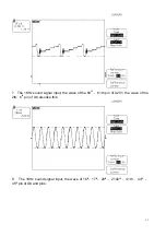
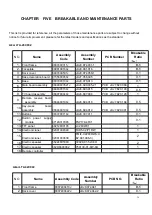
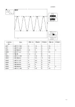
background image

1

2

3

4

A

B

C

D

4

3

2

1

D

C

B

A

Title

Number

Revision

Size

B

Date:

13-Apr-2005

Sheet    of 

File:

E:\USER\MJ\LP08\YLT-chn\LS08_MAIN_TDA8759-20050223.Ddb

Drawn By:

S C L _ V

S C L _ V

2 3 S D C L K

D A C R S T #

2 3 S D W E #

S D A _ V

23SDA9

23SDD27

23SDD25

23SDD23

F L I C L K

23SDA0

23SDD24

23SDD17

23SDD3

DEVADDR0

F L I G R N 2

F L I G R N 4

2 3 S D D 2

2 3 S D A [ 1 0 . . 0 ]

F L I H S

23SDA3

23SDA4

2 3 0 0 O E #

23SDD21

2 3 S D D [ 3 1 . . 0 ]

23SDDQM

23SDD8

2 3 S D D 0

2 3 S D R A S #

F L I V S

F L I G R N 7

23SDD12

23SDD11

23SDD18

23SDD13

2 3 S D D 1

2 3 S D A [ 1 0 . . 0 ]

BDACOUT

RDACOUT

2 3 S D C A S #

23SDA10

23SDD16

23SDD7

23SDD6

23SDD4

F L I H R E F

23SDD26

23SDD19

23SDD5

SDCKO

23SDA2

23SDA7

23SDD30

23SDD22

DEVADDR1

2 3 S D B A 0

F L I G R N 5

23SDA8

23SDD15

23SDD14

2 3 S D D [ 3 1 . . 0 ]

2 3 S D B A 1

F L I G R N 3

23SDA5

23SDA6

23SDD9

GDACOUT

2 3 S D C S #

F L I G R N 6

23SDA1

23SDD29

23SDD28

F L I G R N 0

F L I G R N 1

23SDD31

23SDD20

23SDD10

V G R N [ 7 . . 0 ]

V G R N 0

V G R N 2

V G R N 1

V G R N 6

V G R N 4

V G R N 7

V G R N 5

V G R N 3

DEVADDR0

2 3 0 0 O E #

DEVADDR1

F L I C L K

F L I H S

F L I H R E F

F L I V S

F L I B L U 7

F L I B L U 6

F L I B L U 5

F L I B L U 4

F L I B L U 3

F L I B L U 2

F L I B L U 1

F L I B L U 0

V B L U 3

V B L U 7

V B L U 5

V B L U 2

V B L U 6

V B L U 4

V B L U 1

V B L U 0

V B L U [ 7 . . 0 ]

S D A _ V

C491

47uF/10V

C402

0.1uF

R437

100R/5%

R411

22R/5%

R440

100R/5%

R447

10K/5%

1

TP404

R417

75R/1%

FLI2310

HSYNC1_PORT1

1

VSYNC1_PORT1

2

FIELD ID1_PORT1

3

IN_CLK1_PORT1

4

HSYNC2_PORT1

5

VSYNC2_PORT1

6

FIELD ID2_PORT1

7

VDD1(3.3)

8

VSSio

9

IN_CLK2_PORT1

10

B/Cb/D1_0

11

B/Cb/D1_1

12

B/Cb/D1_2

13

B/Cb/D1_3

14

B/Cb/D1_4

15

VDDcore1(1.8)

16

VSScore

17

B/Cb/D1_5

18

B/Cb/D1_6

19

B/Cb/D1_7

20

R/Cr/CbCr_0

21

R/Cr/CbCr_1

22

R/Cr/CbCr_2

23

R/Cr/CbCr_3

24

R/Cr/CbCr_4

25

R/Cr/CbCr_5

26

R/Cr/CbCr_6

27

R/Cr/CbCr_7

28

G/Y/Y_0

29

VDD2(3.3)

30

VSSio

31

G/Y/Y_1

32

G/Y/Y_2

33

G/Y/Y_3

34

G/Y/Y_4

35

VDDcore2(1.8)

36

VSScore

37

G/Y/Y_5

38

G/Y/Y_6

39

G/Y/Y_7

40

IN_SEL

41

TEST

42

DEV_ADDR1

43

DEV_ADDR0

44

SCLK

45

SDATA

46

RESET_N

47

VDD3(3.3)

48

VSSio

49

SDRAM D0

50

SDRAM D1

51

SDRAM D2

52

SDRAM D3

53

SDRAM D4

54

SDRAM D5

55

SDRAM D6

56

SDRAM D7

57

SDRAM D8

58

SDRAM D9

59

SDRAM D10

60

SDRAM D11

61

VDD4(3.3)

62

VSSio

63

SDRAM D12

64

SDRAM D13

65

SDRAM D14

66

SDRAM D15

67

VDDcore3(1.8)

68

VSScore

69

SDRAM D16

70

SDRAM D17

71

SDRAM D18

72

SDRAM D19

73

SDRAM D20

74

SDRAM D21

75

SDRAM D22

76

SDRAM D23

77

SDRAM D24

78

SDRAM D25

79

VDDcore4(1.8)

80

VSScore

81

SDRAM D26

82

SDRAM D27

83

SDRAM D28

84

SDRAM D29

85

SDRAM D30

86

SDRAM D31

87

VDD5(3.3)

88

VSSio

89

TEST IN

90

SDRAM ADDR10

91

SDRAM ADDR9

92

SDRAM ADDR8

93

SDRAM ADDR7

94

SDRAM ADDR6

95

VDDcore5(1.8)

96

VSScore

97

SDRAM ADDR5

98

SDRAM ADDR4

99

SDRAM ADDR3

100

SDRAM ADDR2

101

SDRAM ADDR1

102

SDRAM ADDR0

103

SDRAM WEN

104

O E

156

G/Y/Y_OUT_7

155

G/Y/Y_OUT_6

154

G/Y/Y_OUT_5

153

G/Y/Y_OUT_4

152

G/Y/Y_OUT_3

151

G/Y/Y_OUT_2

150

G/Y/Y_OUT_1

149

G/Y/Y_OUT_0

148

VSSio

147

VDD8(3.3)

146

R/Y/Pr_OUT_7

145

R/Y/Pr_OUT_6

144

R/Y/Pr_OUT_5

143

R/Y/Pr_OUT_4

142

R/Y/Pr_OUT_3

141

R/Y/Pr_OUT_2

140

VSScore

139

VDDcore7(1.8)

138

R/Y/Pr_OUT_1

137

R/Y/Pr_OUT_0

136

B/U/Pb_OUT_7

135

B/U/Pb_OUT_6

134

B/U/Pb_OUT_5

133

B/U/Pb_OUT_4

132

B/U/Pb_OUT_3

131

B/U/Pb_OUT_2

130

VSSio

129

VDD7(3.3)

128

B/U/Pb_OUT_1

127

B/U/Pb_OUT_0

126

CLKOUT

125

VSScore

124

VDDcore6(1.8)

123

CTLOUT4

122

CTLOUT3

121

CTLOUT2

120

CTLOUT1

119

CTLOUT0

118

TEST OUT1

117

TEST OUT0

116

TEST3

115

SDRAM CLKIN

114

VSSio

113

VDD6(3.3)

112

SDRAM CLKOUT

111

SDRAM DQM

110

SDRAM CSN

109

SDRAM BA0

108

SDRAM BA1

107

SDRAM CASN

106

SDRAM RASN

105

HS_PORT2

208

VS_PORT2

207

FID_PORT2

206

D1_IN_7

205

D1_IN_6

204

D1_IN_5

203

D1_IN_4

202

D1_IN_3

201

D1_IN_2

200

D1_IN_1

199

VSScore

198

VDDcore8(1.8)

197

D1_IN_0

196

IN_CLK_PORT2

195

VSSio

194

VDD9(3.3)

193

XTAL OUT

192

XTAL IN

191

TEST2

190

TEST1

189

TEST0

188

DAC_PVDD(3.3)

187

DAC_GR_AVDD(3.3)

186

DAC_GR_AVSS

185

DAC_AVSS

184

DAC_AVDD(3.3)

183

DAC_VREFIN

182

DAC_VREFOUT

181

DAC_RSET

180

DAC_COMP

179

DAC_AVSSR

178

DAC_AVDDR(3.3)

177

DAC_ROUT

176

DAC_AVSSG

175

DAC_AVDDG(3.3)

174

DAC_GOUT

173

DAC_AVSSB

172

DAC_AVDDB(3.3)

171

DAC_BOUT

170

DAC_VSS

169

DAC_VDD(1.8)

168

DAC_PVSS

167

AVSS_PLL_FE

166

AVDD_PLL_FE(1.8)

165

AVDD_PLL_SDI(1.8)

164

AVSS_PLL_SDI

163

AVSS_PLL_BE2

162

AVDD_PLL_BE2(1.8)

161

AVDD_PLL_BE1(1.8)

160

AVSS_PLL_BE1

159

PLL_PVSS

158

PLL_PVDD(1.8)

157

U401

R439

100R/5%

C471

0.1uF

R409

22R/5%

R449

22R/5%

C487
0.1uF

C490

47uF/6.3V

C474

0.1uF

C492
0.1uF

R410

22R/5%

R416

75R/1%

R434
22R/5%

C472

0.1uF

C476

0.1uF

C405
22uF/6.3V

C479

0.1uF

R445

10K/5%

C4104

22uF/6.3V

C478

0.1uF

C473

0.1uF

C496

0.1uF

C4103

0.1uF

C475

0.1uF

C480

22uF/6.3V

C400

22pF

R432
22R/5%

1

2

FB412

C406
22uF/6.3V

C498

0.1uF

C477

0.1uF

R450

22

C4100

0.1uF

R442

100R/5%

C495

0.1uF

C4102

0.1uF

C4117
0.1uF

GND

1

VIN

3

TAB

4

2

U403
LM1117DTX-1.8

T O - 2 5 2

C4116
0.1uF

L409

5.6uH/5%

C4114
0.1uF

C497

0.1uF

C4112
0.1uF

R446

10K/5%

C403

0.1uF

C499

0.1uF

1

2

3

X400

13.5MHz

C4101

0.1uF

R404

187R/1%

C4115
0.1uF

C4113
0.1uF

L412

5.6uH/5%

C4111
0.1uF

R438

100R/5%

C4105
22uF/6.3V

1

2

FB411

C411 0.1uF

C486

22uF/6.3V

1

TP400

R418

75R/1%

C4118

22uF/6.3V

1

TP403

1

TP402

R401
470K/1%

C4106
0.1uF

1

TP401

L410

5.6uH/5%

VGRN[7..0]

23SDD[31..0]

23SDCLK
23SDDQM
23SDCS#
23SDBA0
23SDBA1
23SDCAS#
23SDRAS#
23SDWE#
23SDA[10..0]

VVS

VCLK

VHS

VBLU[7..0]

DAC3.3V

3.3VS23

1.8VS23

DAC1.8V

PLL1.8V

GND

1.8VS23

DAC3.3V

3.3VS23

DAC1.8V

PLL1.8V

+1.8V_SW

+1.8V_SW

+3.3V_SW

+3.3V_SW

GND

GND

GND

GND

GND

GND

GND

GND

GND

GND

+3.3V_SW

+1.8V_SW

GND

+5V_SW

GND

NOTE: FLI2300 could be used in place of FLI2310

)25 7( 673 85326( ,1 &$6(2) ) /, 21 /<

DECOUPLING FOR FLI2310

+

+

+

+

+

+

+

Leave 1sq inch- exposed copper area attached to Tab of U408

WHEN FLI2310 IS PRESENT

WHEN FLI2310 IS NOT PRESENT

ASSEMBLE RN700  TO RN707.

DO NOT ASSEMBLE RN710, RN711,RN712,RN713

F L I R E D 2

F L I R E D 4

F L I R E D 7

F L I R E D 5

F L I R E D 3

F L I R E D 6

F L I R E D 0

F L I R E D 1

V R E D 7 . . 0 ]

VRED[7..0]

V R E D 0

V R E D 2

V R E D 1

V R E D 6

V R E D 4

V R E D 7

V R E D 5

V R E D 3

ADCLK

ADHS
ADVS

L407

10uH

L406

10uH

+3.3V_SW

3V3A

3V3D

Y400

24.576MHz

C4004

22P

GND

C404
22P

Strapping' Clock

R441

Open

R443
4.7K

C493
100n

C489
100n

C488
100n

C485
100n

C484
100n

C483
100n

C482
100n

C481
100n

C470
100n

C469
100n

C468
100n

C494
100n

C4003
100n

C4001
100n

+ C4002

10u

+C467

10u

GND

GND

3V3A

3V3D

GND

R436
100

C459
47nF

C460
47nF

C461
47nF

C462
47nF

C464
47nF

C465
47nF

C463

47nF

C466
47nF

R420

18R

R421

0

R422

0

R423

0

R424

0

R428
56R

R429
N C R430

N C

R431
N C

R433
N C

R435
N C

Scart2_CIn

Scart2_VideoIn

Video1_C_IN

Video1_Y_IN

SubchannelTV

'Strapping' I2C Slave

ITRU0

ITRU1

ITRU2

ITRU3

ITRU4

ITRU5

ITRU6

ITRU7

ITRU[0..7]

ITRU[0..7]

TCK

98

TMS

99

TDI

3

TRSN

97

TDO

2

VDDA0

23

VDDA1

17

VDDA2

11

VDDE

1

VDDE

25

VDDE

51

VDDE

75

VDDI

33

VDDI

43

VDDI

58

VDDI

68

VDDI

83

VDDI

93

VXDD

8

HPD0

72

HPD1

71

HPD2

70

HPD3

69

HPD4

67

HPD5

66

HPD6

65

HPD7

64

TEST3

77

TEST4

78

TEST5

79

SCL

31

SDA

32

AOUT

22

SAA7115HL

AI24

10

AI23

12

AI22

14

AI21

16

AI2D

13

AI12

18

AI11

20

AI1D

19

CE

27

VSSA0

24

VSSA2

9

VSSA1

15

AGND

21

VXSS

5

VSSE

26

VSSI

38

VSSE

50

VSSI

63

VSSE

76

VSSI

88

VSSE

100

LLC

28

LLC2

29

RESON

30

RTS0

34

RTS1

35

RTCO

36

TEST0

44

TEST1

73

TEST2

74

XPD0

90

XPD1

89

XPD2

87

XPD3

86

XPD4

85

XPD5

84

XPD6

82

XPD7

81

XRI1

92

XRV

91

XCLK

94

XDQ

95

XRDY

96

XTRI

80

XTOUT

4

IPD0

62

IPD1

61

IPD2

60

IPD3

59

IPD4

57

IPD5

56

IPD6

55

IPD7

54

ITRDY

42

ICLK

45

IDQ

46

ITR1

47

IGP0

48

IGP1

49

IGPV

52

IGPH

53

AMCLK

37

ASCLK

39

ALRCLK

40

AMXCLK

41

XTAL

6

XTAL1

7

U402

SAA7115HL

R426

100R/5%

R425

100R/5%

SVCLK

SVCLK

GND

ALRCLK is used to seleted to 24.576MHZ crystal.

SAA7115_EN

REF_B/Pb

49

B/Pb3

50

B/Pb2

51

B/Pb1

52

BIAS

56

REF_G/Y

62

G/Y3

63

G/Y2

64

G/Y1

65

SOG/Y3

72

SOG/Y2

73

SOG/Y1

74

REF_R/Pr

77

R/Pr3

78

R/Pr2

79

R/Pr1

80

H E

95

COAST

102

GAIN

103

C L A M P

104

VSYNC1

105

VSYNC2

106

VSYNC3

107

HSYNC1

108

HSYNC2

109

HSYNC3

110

CKEXT

111

TCLK

113

SDA

118

S C L

119

DIS

114

A0

96

C S

170

ORR/V

171

ORB/U

172

ORG/Y

173

V A I

174

FREF

175

VREF

176

PL

166

D E

167

O E

94

CKP

2

HS

168

VS

169

HREF

1

VP00

7

VP01

8

VP02

9

VP03

10

VP04

15

VP05

16

VP06

17

VP07

18

VP10

23

VP11

24

VP12

25

VP13

26

VP14

27

VP15

28

VP16

31

VP17

32

VP20

35

VP21

36

VP22

39

VP23

40

VP24

41

VP25

42

VP26

43

VP27

44

TDA8795

U400A

TDA8759

C420

10n

R406

75

c4119

10n

c4120

10n

c415

10n

R402

12K

R400 75

c416

10n

c4121

10n

c417

10n

c410

10n

c418

10n

c412

10n

c419

10n

c4122

10n

c413

10n

c414

10n

R403

75

GND

R413

N C

R414

100

R412

100

TV_Csync

GND

R415

4.7K

3.3Vcore

1

2

3

4

5
6
7
8

RN402
47X4

N C

5

N C

6

N C

19

N C

20

N C

33

N C

34

N C

115

N C

128

N C

129

N C

134

N C

135

N C

136

N C

137

N C

140

N C

141

N C

143

N C

144

N C

146

N C

147

N C

149

N C

150

N C

152

N C

153

N C

155

N C

156

Vpll_1.8v

87

Vpll_3.3v

88

Vfro

85

PD

93

Vi2c

123

Vbias

59

Vcca

82

Vcca

76

Vcca

69

Vcca

67

Vcca

61

VccA

54

Vcca

48

Vcore

138

Vcore

139

Vcore

145

Vcore

151

Vcore

157

Vcore

158

Vcore

132

Vcore

130

Vcore

116

Vcore

11

Vp

164

Vp

3

Vp

13

Vp

21

Vp

29

Vp

37

Vp

45

OGND

165

OGND

4

OGND

14

OGND

22

OGND

30

OGND

38

OGND

46

DGND

12

DGND

117

DGND

127

DGND

131

DGND

159

DGND

133

DGND

142

DGND

148

DGND

154

AGND

47

AGND

53

AGND

55

AGND

57

AGND

58

AGND

60

AGND

66

AGND

68

AGND

70

AGND

71

AGND

75

AGND

81

AGND

83

AGND_pll

84

AGND_pll

86

DGNDi2c

120

DGNDi2c

126

TST0

89

TST1

90

TST2

91

TST3

92

TST4

97

TST5

98

TST6

99

TST7

100

TST8

101

TST9

112

TST10

121

TST11

122

TST12

124

TST13

125

TST14

160

TST15

161

TST16

162

TST17

163

TDA8759

U400B

TDA8759

3.3V_out

1.8Vcore

3.3Vcore

3.3Vcca

3.3Vcca

3.3Vcore

1.8Vpll
3.3Vpll

GND

GND

GND

+C457

22u/10V

+C458

22u/10V

C451
0.1uF

+

C442
470u/10V

C427

0.1u

C430
0.1u

C433
0.1u

C436
0.1u

C438
0.1u

C440
0.1u

C443
0.1u

C445
0.1u

C423
0.1u

C425
0.1uF

C428
0.1uF

C431
0.1uF

C434
0.1uF

C437
0.1uF

C439
0.1uF

C422
0.1uF

C424
0.1uF

C426
0.1uF

C429
0.1uF

C432
0.1uF

C447
0.1uF

C448
0.1uF

C449
0.1uF

C452
0.1uF

C453
0.1uF

C455
0.1uF

C454
0.1uF

3.3V_out

3.3Vcca

3.3Vcore

1.8Vcore

1.8Vpll

3.3Vpll

GND

GND

GND

GND

GND

R405 1K

GND

ADUB0

ADUB1

ADUB2

ADUB3

ADUB4

ADUB5

ADUB6

ADUB7

ADYG0

ADYG1

ADYG2

ADYG3

ADYG4

ADYG5

ADYG6

ADYG7

ADVR0

ADVR1

ADVR2

ADVR3

ADVR4

ADVR5

ADVR6

ADVR7

1
2
3
4

5

6

7

8

RN409

22

SubchannelTV

Video1_Y_IN

Scart1VideoIN

Scart2_VideoIn

Scart2_CIn

Video1_C_IN

Scart1VideoIN

R419

0

SAA7115_EN

8759PowerDown

HIGH:

8759Powerdown

8759PowerDown

R408

100

High is effective.

C407
47uF/10V

C409

47uF/6.3V

C408

0.1uF

GND

1

VIN

3

TAB

4

2

U405
LM1117DTX-3.3

T O - 2 5 2

+3.3V_DEC

GND

+5V_SW

Leave 1sq inch- exposed copper area attached to Tab of U408

+3.3V_DEC

+3.3V_SW

L402
10uH

+3.3V_SW

L400
10uH

+3.3V_DEC

L401
10uH

+1.8V_SW

L403
10uH

+3.3V_DEC

L405
10uH

C450
0.1uF

GND

L404
10uH

+1.8V_SW

+ C444

22u/10V

+ C446

22u/10V

+ C435

22u/10V

+ C456

22u/10V

TDA8759 AD Power Supply.

ADYG00
ADYG11
ADYG22
ADYG33
ADYG44
ADYG55
ADYG66
ADYG77

ADUB00
ADUB11
ADUB22
ADUB33
ADUB44
ADUB55
ADUB66
ADUB77

ADVR00
ADVR11
ADVR22
ADVR33
ADVR44
ADVR55
ADVR66
ADVR77

V G R N 0

V G R N 2

V G R N 1

V G R N 6

V G R N 4

V G R N 7

V G R N 5

V G R N 3

V B L U 3

V B L U 7

V B L U 5

V B L U 2

V B L U 6

V B L U 4

V B L U 1

V B L U 0

V R E D 0

V R E D 2

V R E D 1

V R E D 6

V R E D 4

V R E D 7

V R E D 5

V R E D 3

ADCLK

ADHS
ADVS

ADCLK

ADHS
ADVS

1
2
3
4

5

6

7

8

RN411 22X4

VCLK

VHS
VVS

VVS

VCLK

VHS

VCLK

VHS
VVS

When FLI2300 is not installed,where should SHREF be  connected?

DO NOT ASSEMBLE TO RN700  TO RN707.

ASSEMBLE RN710, RN711,RN712,RN713

RESET_2310

RESET_2310

Reset  SAA7115  on the same time.

C401

22pF

TV_Csync

ADYG00

ADYG11
ADYG22
ADYG33
ADYG44

ADYG55
ADYG66
ADYG77

ADUB00
ADUB11
ADUB22
ADUB33

ADUB44
ADUB55
ADUB66
ADUB77

ADVR00
ADVR11
ADVR22
ADVR33
ADVR44
ADVR55
ADVR66
ADVR77

R456

N C

VHS

1

2

3

4

5
6
7
8

RN400A 22X4

1

2

3

4

5
6
7
8

RN410 22X4

1

2

3

4

5
6
7
8

RN410A 22X4

1

2

3

4

5
6
7
8

RN401 22X4

1

2

3

4

5
6
7
8

RN401A22X4

1
2
3
4

5

6

7

8

RN404

22X4

1
2
3
4

5

6

7

8

RN404A

22X4

ADUB00

ADUB11

ADUB22

ADUB33

ADUB44

ADUB55

ADUB66

ADUB77

1
2
3
4

5

6

7

8

RN406

22X4

1
2
3
4

5

6

7

8

RN406A

22X4

ADVR00

ADVR11

ADVR22

ADVR33

ADVR44

ADVR55

ADVR66

ADVR77

1
2
3
4

5

6

7

8

RN408
22X4

1
2
3
4

5

6

7

8

RN408A

22X4

ADYG00

ADYG11

ADYG22

ADYG33

ADYG44

ADYG55

ADYG66

ADYG77

1

2

3

4

5
6
7
8

RN407

22X4

1

2

3

4

5
6
7
8

RN407A 22X4

1

2

3

4

5
6
7
8

RN405

22X4

1

2

3

4

5
6
7
8

RN405A 22X4

1

2

3

4

5
6
7
8

RN403 22X4

1

2

3

4

5
6
7
8

RN403A22X4

S C L _ V

S D A _ V

1

2

3

4

5
6
7
8

RN400 22X4

TP406

TP405

C4123
N C

C4124
N C

C4125
N C

GND

GND

GND

TV_RRout

TV_Rout

R171
470

R176
N C

L171

C174
0.1uF

C172
10V22uF

L172
2.2uH

C171
330pF

C173
330pF

R172
75

VCC5A

R182

100

TV_Rout

Q171
2SC1815Y

TV_BBout

TV_Bout

R173
470

R175
N C

L174
2.2uH

C179
330pF

C180
330pF

R174

75

TV_Bout

R183
100

Q172
2SC1815Y

TV_GGout

TV_Gout

R179
470

R181

N C

L175
2.2uH

C182
330pF

C183
330pF

R180
75

R184
100

TV_Gout

Q173
2SC1815Y

MA1
PP

MA2
PP

MA3
PP

C419A

10n

uoc_vs

R452

47

R451

22

uoc_hs

R406A

75

R400A

75

R403A

75

R175A
75

R181A

75

R176A
75

C494A
100n

P B o u t

Yout

Yout

2

1

3

U404

2N7002E

2

1

3

U406

2N7002E

R454

1K

R455

1k

M S T R _ S C L

M S T R _ S D A

S C L _ V

S D A _ V

R444
4.7K

R453
4.7k

3.3V_out

3.3V_out

Summary of Contents for LTA-26C902

Page 1: ...www akai ru Models LTA 26C902 LTA 32C902 LTA 37C902 ...

Page 2: ...2 ...

Page 3: ......

Page 4: ...computer terminal display equipment Legerity convenience low power consumption Digital Photo Album Function Only for CHD W260F8P CHD W270F8P CHD W320F8P CHD W370F8P Built in DVD Module Only for CHD TD260F8 CHD TD270F8 CHD TD320F8 CHD TD370F8 Entirely Compatible to DVD SVCD VCD CD MP3 Compatible to PAL NTSC Discs High quality digital audio coaxial input enable you to feel as if sit in the theatre w...

Page 5: ...of transforming outer signal into the uniform digital signal identified by LCD display with use of System Control IC TV and AV signals input from TV Board are decoded by UOCIII to transport RGB signal which is to be transformed by TDA8759 modulus to transport 24bit RGB digital signal then it is to be transformed by GM1601 GM1501 to produce LVDS signal displayed on the screen in addition signals in...

Page 6: ...TV conveniently and know its current working status simply with a remote control 4 Built in Power Board Assembly It can transform AC 220V into DC for ICs including 24V 12V 5V and 5VS power supply in standby mode 5 K Board Assembly It consists of 7 function buttons by which users can operate the TV freely 6 Screen Assembly Screens for LS08 have the built in adverse transformer which change DC into ...

Page 7: ...700 GM1501 BD Video processor 11 U201 TDA15063H N1B06557 AV decoder 12 U402 SAA7115HL V1 Sub channel video decoder 13 U305 SM5302AS G ET High definition signal filter 14 U400 TDA8759HV 8 C1 Video signal modulus transformer 15 U5 TDA9178T N1 Video signal picture amendment 16 U600 MT46V2M32LG 4 Frame buffer ICs FUNCTION INTRODUCTION IN DETAILS Main Tuner TMI4 C22P2RW Pin Definition Description 1 AGC...

Page 8: ...ge catch process and clock display It integrates high velocity AD converter PLL high reliability DVI receiver X86 series miccontrol and LCDS inverter See the features as below Main Features High quality image zoom function Analog RGB signal input interface Intelligent output signal auto identification Integrated high power PLL output High reliable self adaptive DVI input interface 4 4 4 4 2 2 CCR6...

Page 9: ...8 B10 RX0 RX2 RX0 RX2 DVI input port B11 REXT Exterior exit resistance C6 C11 DVI 3 3 DVI 3 3V power supply D6 D8 D10 DVI 1 8 DVI 1 8V power supply A7 A11 B5 B7 C7 D7 D11 DVI GND DVI ground Low Bandwidth ADC Port C13 LBADC 33 ADC3 3Vpower supply A12 B12 C12 LBADC_IN1 LBADC_IN3 ADC analog input channel D12 LBADC_RETURN Channel analog ground D13 LBADC GND Power supply voltage analog ground OCM IC Po...

Page 10: ...Pr signal input B23 B24 B25 A24 A25 C23 C24 D24 VBLU7 VBLU0 Blue signal or U Cb Pb signal input Screen Control Port A26 PPWR Screen power control B26 PBIAS Screen bias control D26 C25 C26 PWM2 PWM0 Pulse width modulation output AC7 DCLK Pels clock output AC16 OEXTR Connect external LVDS bias resistance LVDS Port AE14 AE16 AE19 AE23 AF13 AF16 AF19 AF23 AF11 A0 A3 A0 A3 B0 B3 B0 B3 Low voltage diffe...

Page 11: ...4 EXTCLK External clock input Frame Storage Interface U24 U23 FSCLKp FSCLKn Fine storage clock output V24 V25 FSRAS FSCAS Address output V26 FSWE Write enable port W26 FSCKE Read enable port J24 FSVREF Reference voltage input K26 FSVREFVSS Reference voltage ground W25 FSVREF Reference voltage input W24 FSVREFVSS Reference voltage ground L26 FSDQS Data filter F24 F26 G23 G26 H24 H26 J25 J26 R24 R26...

Page 12: ...ply K12 K13 K14 K15 L10 L12 L13 L14 L15 L17 M10 M11 M12 M13 D_GND Power ground A1 AC D5 AC17 K3 F1 NO_CONNECT NC GM1501Internal Diagram TDA8759 TDA8759 is a triple 8 bit video converter interface The IC converts a RGB analog signal into a 24bit RGB or YUV or YCbCr digital signal or converts a YUV or YCbCr analog signal into a YUV or RGB digital signal with a sampling rate up to 81 Msps The IC supp...

Page 13: ...h temperature Output format RGB 4 4 4 YUV 4 4 4 YUV 4 2 2 CCIR 656 or YUV 4 2 2 semi planar standard on output bus I C bus control Programmable clock phase adjustment cells Amplifier bandwidth of 100 MHz Integrated PLL divider Power Downmode TDA8759 Internal Diagram Pin Description Pin Name Description 1 HREF Horizontal reference output 2 VCLK Video clock output 3 13 21 29 37 45 164 VDDO Video por...

Page 14: ... on green brightness channel input 77 REFR Pr Red red chrominance channel reference input 80 79 78 R Pr1 R Pr3 Red red chrominance channel analog input 89 92 97 101 112 121 122 124 125 160 163 TST0 TST17 Reserved for test 93 PD Power down control input 94 OE Output enable input 96 A0 I C bus address control input 102 COAST PLL control input 103 GAIN Gain input 104 CLAMP Clamp input 105 107 VSYNC1 ...

Page 15: ... Description 26 30 AGND Analog ground for digital analog cells in core 33 AVCC High voltage analog power supply 8 14V 29 AVDD 5V regulated output capable of 100mA output 7 AVDDREF Reference 5V output 13 BSLN 24 BSLP Bootstrap I O left channel 48 BSRN 37 BSRP Bootstrap I O right channel 28 COSC I O for charge discharge currents onto capacitor for ramp generator triangle wave 6 LINN 5 LINP Negative ...

Page 16: ...nput for right channel 27 ROSC Current setting resistor for ramp generator Nominally equal to 1 8 44 45 40 41 ROUTN ROUTP Class D 1 2 H bridge negative output for right channel ROUTP 40 41 O Class D 1 2 H bridge positive output for right channel 1 SD Shutdown signal for IC low shutdown high operational TTL logic levels with compliance to VCC 9 VARDIFF DC voltage to set the difference in gain betwe...

Page 17: ... difference and phase difference values Main Features supply voltage 5V 10 _DC voltage level restore sync clamp function Output buffer gain switching function 0 6dB input to output AC signal gain Channel to channel gain difference 0 5dB 5 supply voltage variation Channel to channel phase difference 3 5 degree Output signal harmonic distortion all channels 1 5 Cutoff frequency 5 8 to 37MHz variable...

Page 18: ...set input 9 DISABLE Power save function Built in pull down resistor 10 13 16 19 GND Ground 11 BOUT VOUT B V signal output 14 GOUT UOUT Analog 5V supply 17 ROUT YINB R Y signal output 12 15 18 24 VCC Analog 5V supply 20 RFC LPF lowpass filter cutoff frequency setting resistor connection 21 VFC LPF lowpass filter cutoff frequency setting voltage input 22 MUXSEL Input select signal 23 SYNCIN Filter c...

Page 19: ...ors Two improved 9 Bit CMOS analog to digital converter in differential CMOS style Automatic Clamp Control ACC for CVBS Y and C Enhanced Horizontal and vertical Sync Detection PAL delay line for correcting PAL phase errors Automatic TV VCR detection SAA7115 Internal Diagram Pin Function Pin Name Description 1 8 11 17 23 25 33 43 51 58 68 75 83 93 VDD Supply voltage port 2 TDO Test Data Output for ...

Page 20: ...or backward compatibility do not use for new applications 30 RESON RESet Output Not signal 31 SCL IIC serial clock line with inactive output path 32 SDA IIC serial data line 34 RTS0 35 RTS1 real time status or sync information controlled by subaddr 11h and 12h RTS1 35 O real time status or sync information controlled by subaddr 11h and 12h 36 RTCO Real time control output 37 AMCLK Audio master clo...

Page 21: ...O expansion port 95 XDQ data qualifier I O expansion port 96 XRDY task flag or read signal from scaler controlled by XRQT subaddr 83H 97 TRSTN Test ReSeT Not for Boundary Scan Test with internal pull up for board design without Boundary Scan connect TRSTN to ground 1 98 TCK Test Clock for Boundary Scan Test with internal pull up 2 99 TMS Test Mode Select for Boundary Scan Test or Scan Test with in...

Page 22: ...can be demodulated For the QIP90 versions this is valid only for the stereo versions Built in adaptable brightness delay circuit switchable brightness signal transmission rate Pin Description Pin Name Description 1 2 12 18 28 40 68 81 89 92 95 101 121 125 VSS GND ground 3 4 45 69 82 88 90 91 93 94 96 100 110 117 118 124 VDD Power supply 5 VREF_POS_LSL 6 VREF_NEG_LSL HPL 7 VREF_POS_LSR HPR 8 VREF_N...

Page 23: ...voltage TV processor 5 V 48 IFVO SVO CVBSI video output selected CVBS output CVBS 49 AUDIOIN4L 50 AUDIOIN4R audio 4 input left signal audio 4 input right signal 51 CVBS4 Y4 CVBS Y input 52 C4 chroma 4 input 53 AUDIOIN2L SSIF 54 AUDIOIN2R 56 AUDIOIN3L 57 AUDIOIN3R 30 AUDOUTLSL 61 AUDOUTLSR 62 AUDOUTHPL 63 AUDOUTHPR Audio input 58 CVBS3 Y3 CVBS Y input 59 C2 C3 chroma 2 3 input 55 CVBS2 Y2 CVBS Y in...

Page 24: ...upt 0 or port 0 5 4 mA current sinking direct drive of LEDs 98 99 102 109 111 116 119 120 122 123 126 128 P0 0 P0 4 P1 0 P1 7 P2 0 P2 5 P3 0 P3 3 Data port UOCⅢ Internal Diagram CHAPTER THREE SIGNAL FLOW ANALYSIS AND KEY POINT MEASURE DATA The chapter mainly introduces the receipt and dispose of the AV signal the power supply system and system control process of this TV Signal Flow Analysis 1 Vide...

Page 25: ...ng sound intermediate frequency signal SIF is sent into UOC for demodulation and sound dis Ⅲ posal then the output audio signal is zoomed in by D class TPA3002D2PHPR and is sent into the speaker at last AV companying sound the audio signal input by AV is directly disposed by UOC and zoomed in Ⅲ by TPA3002D2PHPR then transported to the speaker After the companying sound of PC DVI YPbPr are selected...

Page 26: ...26 The composition and distribution of the TV power supply please see the next page ...

Page 27: ...7 3 3V 0 3 3 5 3 3 UP6 LM2596 5 0 24 5 0 5 0 U405 LM1117 3 3 0 3 3 5 3 3 U3 78M08 12 0 8 U403 LM1117 1 8V 0 1 8 5 1 8 U503 LM1806 3 3 0 3 3 5 3 3 U505 LM1117 2 5 0 2 5 5 2 5 U506 LM1117 3 3 0 3 3 5 3 3 U501 LM2596 5 0 12 5 0 5 U502 LM2596 5 0 24 5 0 5 0 U504 LM1117 1 8V 0 1 8 5 1 8 Main Components and Socket Locations and Definitions ...

Page 28: ...scription 1 JP5 TV plane 2 JP2 Side AV 3 JP6 DVD AV output 4 JP7 Speaker 5 JP8 loudhailer 6 JP4 DVD decode board 7 JP3 outside AV input 8 JP9 Up screen screen inverter input 9 JP10 Up screen screen inverter input 10 JP12 power supply plane GND GND GND 12V 12V 12V ...

Page 29: ...HV 8 C1 Video signal AD converter C U402 SAA7115HL V1 Sub channel video decoder D U600 MT46V2M32LG 4 Frame buffer memorizer E U700 GM1601 GM1501 BD Video processor F U305 SM5302AS G ET HD signal filter G U801 AM29LV800DT 70EC Flash the TV control procedure put in it H U6 TPA3002D2PHPR Audio PA I U5 TDA9178T N1 Video signal image improve J K202 K9352N Sound surface filter K K201 K7262N Sound surfac...

Page 30: ...85 Pin86 Pin87 of U201 output R G B signal wave the E pole wave of Q171 Q172 Q173 3 RF input color stripe signal I C bus clock signal UOCIII_SCL the wave of the 98P th P pin of U201 the 11P th P pin of U5 the 4P th P pin of parent sub RF tuner ...

Page 31: ...he 22th pin of U201 the 105P th P pin of U400 5 RF input color stripe signal UOC vertical sync signal the wave of the 22th pin of U201 the 105P th P pin of U400 RF input color stripe signal UOC vertical sync signal the wave of the 22th pin of U201 the 105P th P pin of U400 ...

Page 32: ...32 6 RF input gray ladder signal the TV signal wave in the 19P th P pin of SAA7115 The wave in the 10P th P of SAA7115 also like this ...

Page 33: ...al input the wave of the 60P th P 61th pin of U201 the wave of the 2th 6P th P pin of U6 also like this 8 The 1KHz sound signal input the wave of 16P th P 17P th P 20P th P 2140P th P 41th 44P th P 45P th P pin of U6 and pins ...

Page 34: ... LM1117 3 3V 0 3 3 5 3 3 UP6 LM2596 5 0 24 5 0 5 0 U405 LM1117 3 3 0 3 3 5 3 3 U3 78M08 12 0 8 U403 LM1117 1 8V 0 1 8 5 1 8 U503 LM1806 3 3 0 3 3 5 3 3 U505 LM1117 2 5 0 2 5 5 2 5 U506 LM1117 3 3 0 3 3 5 3 3 U501 LM2596 5 0 12 5 0 5 U502 LM2596 5 0 24 5 0 5 0 U504 LM1117 1 8V 0 1 8 5 1 8 ...

Page 35: ... 24LC21 Symptom Two No picture but sound on LOGO when turning on the TV background light is bright Reason and Resolve Check the connect line in up screen and connect the line Symptom Three No picture no sound no snowflake in TV mode but AV is normal Reason and Resolve Check the outside of high frequency also bus and power supply there is no problem but no output from high frequency so the tuner is...

Page 36: ...B JUJ7 820 088 1 7 8669300150J JUJ6 693 015 PCB JUJ7 820 103 0 5 8 TV board assembly 8669700040J JUJ6 697 004 PCB JUJ7 820 128 1 9 Remote receive board assembly 8669400180J JUJ6 694 018 PCB JUJ7 820 104 0 5 10 Key press board assembly 8669400190J JUJ6 694 019 PCB JUJ7 820 091 0 5 11 Buttons 8833700110J JUJ8 337 011 0 1 12 Built in power supply module 67128017905 FSP179 4F01 0 1 13 TFT panel 682126...

Page 37: ...289100454B TAD5 C2IP1RW 1 16 Electric speaker 56224605080 Y2929 01 5W 8Ω 2 17 Electric speaker 562D6608082 Y50138 01 8W 8 Ω 2 18 Remote controller KLC5A 1 A k a i L T A 3 7 C 9 0 2 NO Name Assembly Code Assembly Number PCB NO BBreakable Ratio 1 Frame 8807400430J JUJ8 074 043 0 1 2 Back cover 8807400442J JUJ8 074 044 2 0 1 3 Base 8807000160J JUJ8 070 016 0 1 4 Main board assembly 8669000354J JUJ6 6...

Page 38: ...de menu After entering into factory mode menu sign of the factory menu M will appear factory menu and setup 1 factory menu display is below M Index 1 HWUC_BRI 0x1F The M denotes entering into factory mode now the figures of index denotes the index number now the HWUC_BRI denotes the name of adjusting item now the 0X1F denotes the numerical value 2 Each adjusting item have only one index number the...

Page 39: ...f not necessary please do not adjust it the items of index number 1 2 3 4 5 6 are not necessary to adjust Adjustment methods for factory menu 1 Select the adjusting item You can skip to the adjusting items by pressing the number key also can select the adjusting item in the order of P P when pressing the number key if the adjusting item is 1 9 input the corresponding number keys and press down OK ...

Page 40: ... AutoColor 2 White balance color temperature adjustment Requisite Meter CHROMA 7120 color analyze instrument or same function instrument contain color coordinate chroma diversion card one White balance adjusting frock request the video output range 0 1V is adjustable 750hm load one Prepare A connect all equipments switch the condition of LCD TV to AV B Set the picture of LCD TV for standard condit...

Page 41: ...lor temperature and color coordinate are contented for above request you should judge the exist of color windage phenomenon namely the value of Δuv is 0 or not If Δuv is not 0 readjust R G B value to 0 and meet color coordinate request ...

Page 42: ...19 VGA_SCL MSTR_SCL SVCLK FSCLK FSCAS RXC OCMDATA 0 7 GREEN ITRU 7 0 RED MSTR_SDA BLUE BLUE ROM_CS RX1 PBIAS DVI_SCL FSWE RX1 DVI_SDA FSCKE VGA_SDA FSDQS RX2 FSBKSEL1 FSCLK RX2 FSBKSEL0 FSDATA 0 31 RX0 AVS RX0 PPWR RED SOG FSDQM 0 3 OCM_RE FSADDR 0 11 VGA_CAB DVI_CAB PWM3 VCLK VVS VHS SEC_SDA SCRT2 FSEL CC_INT1 RGB YPbPr_SEL POWER_OFF VRED 7 0 VGRN 7 0 VBLU 7 0 ITRU 7 0 SVCLK Set_tristate2 Set_tri...

Page 43: ...gnal SPDIF Scart1_R Scart1_G Scart1_B Scart1VideoIN To GM1601 Board ToUOCIII TunerBoard Tuner_IF UOC_SW1 UOC_SW2 AGC UOCIII_SDA UOCIII_SCL UOC_SW1 UOC_SW2 MM_SCL MM_SDA 1 2 3 4 5 6 7 8 9 10 11 12 13 14 15 16 17 18 19 20 21 22 23 24 25 26 27 28 29 30 31 32 33 34 35 36 37 38 39 40 41 42 43 44 45 46 47 48 49 50 JP5 SDA 7166102050 UOCIII_SDA UOCIII_SCL 5VB AVS2 SC2_RIN AVS1 FBLIN1 12V_dc SC1_BIN SC1_G...

Page 44: ...V47uF L202 10uH C214 10nF L213 10uH C231 10V47uF R221 390 C273 50V220nF C247 0 1uF C217 0 1uF C223 0 1uF C220 10V47uF R217 1K L209 10uH R235 100 C256 0 1uF C260 0 1uF C252 2 2uF R236 100 L204 10uH C224 0 1uF L210 10uH C230 10V47uF C225 0 1uF C279 10V10uF C280 0 1uF C278 0 1uF L216 10uH R213 47K C240 50V220nF C241 2 2uF C236 2 2uF C281 22pF C282 22pF C264 0 1uF C266 10V100uF C261 0 1uF R205 100 C23...

Page 45: ... indicate output is set to tristate Set_tristate1 ChannelSel2 ChannelSel1 GND COMB 3 NO0B 1 GND 8 NO3B 4 VEE 7 NO2B 5 Inhibit 6 NO1B 2 ADDA 9 ADDB 10 NO3A 11 NO0A 12 COMA 13 NO2A 14 NO1A 15 VCC 16 U308 NLAS4052 Teltext_HS Teltext_VS GND Sel_HsVs Low Select VGA HS VS High Select TeltextHSVS 1 2 3 4 5 6 7 8 CN303 CON8 1 2 3 4 5 6 7 8 CN304 CON8 Tel_SCL Tel_SDA Teltext_MUTE Teltext_R Teltext_G Teltex...

Page 46: ..._3 3 Y4 D_GND T14 D_GND K15 D_GND N15 D_GND T15 D_GND M16 D_GND N16 D_GND R16 D_GND R12 D_GND K13 D_GND P13 D_GND U13 D_GND M14 D_GND R14 FS_2 5 H23 FS_2 5 J23 FS_2 5 M23 FS_2 5 P23 FS_2 5 L23 FS_2 5 T23 FS_2 5 V23 FS_2 5 R23 FS_2 5 Y23 FS_2 5 AA23 FS_2 5 AB23 FS_2 5 AC23 FS_2 5 W23 FS_2 5 F23 D_GND P11 D_GND M10 D_GND M17 D_GND P17 D_GND R17 D_GND P10 D_GND L17 LVDSB_3 3 AC12 LVDSB_3 3 AD12 LVDSB...

Page 47: ...5 NC Scart2_CIn Scart2_VideoIn Video1_C_IN Video1_Y_IN SubchannelTV Strapping I2C Slave ITRU0 ITRU1 ITRU2 ITRU3 ITRU4 ITRU5 ITRU6 ITRU7 ITRU 0 7 ITRU 0 7 TCK 98 TMS 99 TDI 3 TRSN 97 TDO 2 VDDA0 23 VDDA1 17 VDDA2 11 VDDE 1 VDDE 25 VDDE 51 VDDE 75 V D D I 33 V D D I 43 V D D I 58 V D D I 68 V D D I 83 V D D I 93 VXDD 8 HPD0 72 HPD1 71 HPD2 70 HPD3 69 HPD4 67 HPD5 66 HPD6 65 HPD7 64 TEST3 77 TEST4 78...

Page 48: ...V 3 3V_ADC 1 8V_ADC 2 5V_DDR 5V 5V GND 3 3V_ADC 1 8V GND 3 3V 5V GND 1 8V GND 3 3V_ADC 3 3V_DVI 1 8V_CORE GND 3 3V_PLL 3 3V_DIG 1 8V_DVI GND 5V GND Panel_Power 3 3V_SW GND GND GND 5V_ANG 3 3V_LVDS 3 3V_LVDSA 3 3V_I O_BGA 3 3V_ADC 3 3V_LVDSB 3 3V_ADC 3 3V_LBADC 5V_SW 3 3V_ADC 3 3V_ADC 3 3V_ADC 1 8V 3 3V_ADC 3 3V_ADC 3 3V Leave1sqinch exposedcopperareaattachedtoTabofU903 Leave1sqinch exposedcopperar...

Page 49: ... 10n CA36 0 1u CA41 10n CA50 1u RA54 120K CA52 220P CA51 100n CA10 10u CA34 0 1u CA49 1u CA39 10n LA1 33uH CA25 0 1uF CA24 0 1uF CA38 10n LA2 33uH 1 2 JP7 CON2 LA4 33uH CA28 0 1uF CA26 0 1uF LA3 33uH 1 2 JP8 CON2 CA35 0 1u CA55 0 1u CA37 220uF 16V CA33 0 1u 12V_AUDIO 12V_AUDIO 12V_AUDIO 12V_AUDIO MOL MOR CA42 0 47uF CA43 0 47uF MUTE MUTE 12V_AUDIO 5VE BYP 1 GND 2 SD 3 IN2 4 VO2 5 AVDD 6 VO1 7 IN1 ...

Page 50: ...3 BA0 22 BA1 23 RAS 19 CAS 18 CS 20 WE 17 CLK 68 CKE 67 NC 14 NC 21 DQ16 31 DQ17 33 DQ18 34 DQ19 36 DQ20 37 DQ21 39 DQ22 40 DQ23 42 DQ24 45 DQ25 47 DQ26 48 DQ27 50 DQ28 51 DQ29 53 DQ30 54 DQ31 56 DQM0 16 DQM1 71 DQM2 28 DQM3 59 VDDQ 55 VDDQ 75 VDDQ 81 VDD 43 VSSQ 52 VSSQ 78 VSSQ 84 VSS 44 U601 MT48LC2M32B2TG 5 C608 0 1uF R603 150 140 C622 0 1uF CKE 53 CLK 55 CS 28 CAS 26 RAS 27 WE 25 DM0 23 DM1 56...

Page 51: ...W0 UOC_SW1 AGC SubchannelTV CIN YIN Y Pb Pr YPbPr_L YPbPr_R RIN LIN AV_VOUT VIN AVOUTL AVOUTR 26 27 28 29 30 31 32 33 34 35 36 37 38 39 40 41 42 43 44 45 46 47 48 49 50 J1B 50PIN_12 2 3 7 6 1 4 5 JPY1 AV 1 3PKA AVOUTL AVOUTR RA38 12k RA34 6 8k RA37 12k RA40 6 8k 12V_dc CA28 100uF CA29 0 1uF RA39 1k RA35 1k CA26 10uF CA27 10uF CA24 10uF CA25 10uF RA36 100 12V_PORT LOUT ROUT 12V_dc RA51 10K AV_VOUT ...

Page 52: ...hn LS08 CHINA 0923 ddb 辅板 Drawn By R1 27K R2 10K R4 4 7K R6 1K R3 10K R5 4 7K R7 1K 1 2 3 4 JK1 CN 4 GND GND KK1 SOURCE KK2 MENU KK3 VOL KK4 VOL KK5 CH KK6 POWER KK7 CH NO KEY PRESS 3V 3 3v 0 3V 1 2V 2 0V 0 0 8v CH 0 81 1 6v CH 1 61 2 6v VOL 0 3V 1 2V 2 0V 2 67V 0 0 8v STANDBY 0 81 1 6v VOL 1 61 2 3v MENU 2 3 3 0 source ...

Page 53: ...mber Revision Size B Date 13 Apr 2005 Sheet of File E USER MJ LP08 YLT chn LS08 CHINA 0923 ddb 辅板 Drawn By CK2 0 1UF CK1 16V 47U LK1 22UH 1 2 3 GREEN RED L1 LIGHT 1 2 3 4 5 JK2 CN 5 3 3V_DIG GND 2 OUT 3 Vs 1 UK1 HS0038A2M3V 3 3V_DIG LED2 IRDATA LED1 ...

Page 54: ...R3 82 C6 330pF L2 3 3uH SVIDEO C IN R13 10k R14 10k R21 330 R4 82 R6 10K R9 10K R8 10k R2 82 R16 1K R18 1K C13 0 1uF 5VOUT 5VOUT R7 10k R17 1K R11 10K EARPHONE L EARPHONE R PH SW 5VOUT AUDIO L IN AUDIO R IN R10 10K AUDIO L IN AUDIO R IN R22 47 Q1 2SC2712C Q4 2SC2712C Q5 2SC2712C Q2 2SC2712C Q3 2SC2712C C8 16V 10U C7 16V 10U C12 16V100U 5V 5V 5V 5V 5V 2 3 7 6 1 4 5 12 C 8 9 10 Y 11 K 13 S J3 AVW133...

Page 55: ...JP9 CON 14 1 2 3 4 5 6 7 8 9 10 11 12 13 14 JP10 CON 14 24V_4A 24V_4A Backlight_on_off CP26 0 1uF For panel supply ForGM1601Boardsupply 5V_4A 1 2 3 4 5 6 7 8 J171 NC State SDA IRDATA SCL CP13 470uF CP4 0 1uF Backlight_on_off Backlight_on_off DVD_On Off IRDATA SCL State SDA RP2 22k RP6 nc RP5 nc 5VB GND 1 OUT 2 VIN 3 4 4 UP7 LM1117 1 8V CP23 0 1uF GND V1_8ANA GND 5VB CP20 0 1uF GND CP22 47uF GND P_...

Page 56: ...LOW 11 LOW set all display output to 0 17 LOW 8bit bus with OCM access external ROM 13 LOW disable serial interface debug 15 LOW 18 HIGH 12 LOW 10 LOW Use TCLK 14 LOW BOOTSTRAP HEADER OPEN 1 SHUNTED 0 16 HIGH use crystal 8 bit_flash1 8 bit_flash3 INT_OSC 8 BIT_FLASH2 Custom1 Custom2 Serial Interface Debug1 Serial Interface Debug2 Serial Interface Debug3 OCMADDR 0 19 OCMDATA 0 7 1 2 3 4 5 6 7 8 RN8...

Reviews: