background image

Summary of Contents for PDP4210EA1

Page 1: ......

Page 2: ...erations Circuit Description Main IC Information Panel Information Spare Part List Exploded View If you forget your V Chip Password Software Upgrade This manual is the latest at the time of printing a...

Page 3: ...k of electric shock to persons The exclamation point within an equilateral triangle is intended to alert the user to the presence of important operating and maintenance servicing instructions in the l...

Page 4: ...way from high voltage or high tempera ture components 8 Before returning the set to the customer always perform an AC leakage current check on the exposed metallic parts of the cabinet such as antenna...

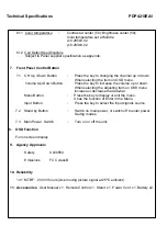
Page 5: ...lor set at Center 50 1 8 Power input 120Vac 60Hz 1 9 Ambient temperature 20 C 5 C 68 F 9 F 1 10 Display mode 31 5KHz 60Hz Resolution 852 x 480 1 11 Other conditions 1 11 1 With image sticking protecti...

Page 6: ...3 2 Aspect Ratio 16 9 3 3 Pixel Resolution 852x480 3 4 Peak Brightness 1500 cd m Panel module without filter 3 5 Contrast Ratio Dark room 10000 1 Panel module without filter 3 6 Viewing Angle Over 160...

Page 7: ...V7 6 2 Size 42 1005mm width x597mm height x61mm depth 1 mm 6 3 Aspect ratio 16 9 6 4 Viewing angle Over 160 6 5 Resolution 852x480 6 6 Weight 14 7kg 0 5 kg Net 1EA 6 7 Color 1073 7 million colors by c...

Page 8: ...ting item on OSD menu increase or decrease the data bar Menu Button Press the key to display or exit the menu It has the function of Enter in the Menu Input Button Press the key to select the input si...

Page 9: ...Multi channel TV sound MTS options Mono Stereo and SAP Second Audio Program Enter Press to move the on screen cursor To select an item press Enter to con rm Exit Press this button to exit Menu Press...

Page 10: ...indicated inside Replace the cover and slide in reverse until the lock snaps P Mode Press repeatedly to cycle through the picture mode Cinema Normal Vivid Hi Bright and User System Press repeatedly t...

Page 11: ...Horizontal Frequency KHz Vertical Frequency Hz 640 x 480 31 50 60 00 37 86 72 81 800 x 600 35 16 56 25 37 90 60 32 46 90 75 00 48 08 72 19 1024 x 768 48 40 60 00 Resolution Horizontal Frequency KHz Ve...

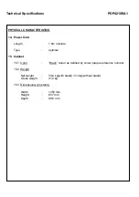
Page 12: ...al 15 Cabinet 15 1 Color Black colour as defined by colour plaque reference number 15 2 Weight Net weight 33 6 kg with stand 31 4kg without stand Gross weight 41 0 kg 15 3 Dimensions w o stand Width 1...

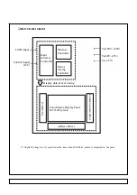
Page 13: ...els Address Driver Scan Driver Common sustain driver Display data Driver timing Memory Controller Driver Timing Controller Input Interface Controller Vcc 5V Va 60V 65V Vs 180V 190V I2C Applied Voltage...

Page 14: ...ocument Number Rev Date Sheet of ZhongShan KAWA Electronic Inc Drawn Checked AKAI_MT8202_MT5351_V1 0 1 C 1 2 Friday March 17 2006 MT5351 Block KAWA Confidential Designer Checker ATSC SYSTEM MT5111 DTV...

Page 15: ...o in YPbPr2 Audio in S_Video Audio HEF4052 U52 MT8202 U12 Video 0 23 data audio signal control signal From MT5351 J24 74LVC244A U30 U33 BUFFER UART0 Communication with MT5351 VGA EEPROM 24C02 U53 VGA_...

Page 16: ...Circuit Diagram Power supply board of PDP Module 1H273W Main Video board Audio Tuner board ATSC board Keypad board Remote control receiver board External L R Speakers board Remote control board...

Page 17: ......

Page 18: ......

Page 19: ...SB33B SB33B 5VSB SB33B SB33B 5V 6V 12V 12V VCC 5VSB SB33B 5VSB J23 DIP7 W H P2 54 1 2 3 4 5 6 7 D26 1N4001 SMD R635 10k NC R57 1K Q19 2N3904 SOT23 SMD 1 3 2 C4 1uF FB39 FB NC R675 100 R776 10k C153 10...

Page 20: ...CB9 0 1uF CE81 100uF 16v CB22 0 1uF CB187 0 1uF CE11 100uF 16v U4 AZ1117 adj SOT223 SMD 1 2 3 ADJ GND OUT IN U7 AZ1117 3 3V SOT223 SMD 1 2 3 ADJ GND OUT IN L6 FB U37 AZ1117 adj SOT223 SMD 1 2 3 ADJ G...

Page 21: ...GPIO18 8 DV25A 5 SDV25A 5 CCIR_V5 8 SCL_8202 6 9 12 SDA_8202 6 9 12 A_CKE 5 A_CAS 5 A_DQS 0 3 5 A_CLK 5 A_WE 5 A_BA 0 1 5 A_RA 0 11 5 VREF 5 A_CS 5 A_DQ 0 31 5 A_RAS 5 A_DQM 0 1 5 A_CLK 5 F_D 0 7 5 F_...

Page 22: ...FE0 3 AVDD_VAD0 3 AADCVDD 3 ADACVDD 3 VPLLVDD2 3 LVDDA 3 AVDD_VAD1 3 AVDD_VFE1 3 PLLVDD1 3 PLLVDD2 3 PLLVDD3 3 XTALVDD 3 VPLLVDD1 3 DACVDDA 3 DACVDDB 3 DACVDDC 3 TESTP3 3 TESTN3 3 LVDDB 3 PWM2VREF 3 A...

Page 23: ...B123 0 1uF R68 47 CB101 0 1uF CB93 0 1uF CB110 0 1uF CB80 0 1uF U17 29LV160 25 24 23 22 21 20 19 18 8 9 28 47 16 29 31 33 35 7 26 38 40 42 44 30 32 10 36 39 41 43 45 37 27 11 15 34 46 6 4 5 3 2 1 48 1...

Page 24: ...IP3 W H P2 0 1 2 3 U34 UPA672T 1 2 3 4 5 6 S1 G1 D2 S2 G2 D1 TP61 RN28 33x4 1 2 3 4 5 6 7 8 R692 4 7K TP60 CB210 0 1uF L84 FB TP70 CB224 0 1uF C629 1000PF R709 47k C616 1000PF MT8293 U25 MT8293 LQFP12...

Page 25: ...TXD 3 11 CCIR_V6 3 GPIO3 3 SDA0 3 SCL0 3 9V 1 9 14 SB33B SB33B SB33B SB33B VCC 9V SB33B VCC DV33B SB33B R357 0 CE142 220uF 16v NC R4 0 R363 1K NC R229 0 R354 0 NC C602 1uF NC CE143 220uF 16v NC R1 10K...

Page 26: ...9 YQ_GND 10 YQ 10 CRQ 10 9V 1 7 9 14 ADC_IN0 3 CCIR_V0 3 SB33B VCC DV33B VCC VCC VCC VCC SB33B 3 3V SWV9 SWV9 SWV9 SWV9 SWV9 SWV9 SWV9 SWV9 SWV9 SB33B SB33B VCC SB33B 5VSB R447 0 NC C156 1000pF NC CE...

Page 27: ...50 100 R666 22k R430 75 1 R409 100k CB196 0 1uF CE132 10uF 25v CE125 10uF 25v R426 0 R402 100k R644 470 R413 1k R652 0 R51 0 NC C183 100pF TP53 R651 39K QF1 MOSFET N 2N7002 SOT23 SMD 1 3 2 CE119 10uF...

Page 28: ...Y1 CVBS_1 CVBS_2 SY_0 SY_1 SC_1 SOY0 3 SOY1 3 Y1_INB 15 Y1_GNDB 8 15 CR1_INB 15 CR1_GNDB 8 15 CB1_INB 15 CB1_GNDB 8 15 CBQ 8 CRQ 8 SC_0_GND 15 YQ 8 YQ_GND 8 CBQ_GND 8 CRQ_GND 8 SY1 3 SY0 3 SC1 3 SC0 3...

Page 29: ..._PLUGPWR SB33B 5VSB 5VSB VCC VCC VCC VGA_PLUGPWR VGA_PLUGPWR VCC VCC R132 68 R159 47K R L P2 RCA1X2 AV2 8 4 13P 1 3 2 C641 0 1uF R736 10K R333 510 C639 0 1uF C636 20pF D73 DIODE SMD BAV99 1 3 2 R16 0...

Page 30: ...1 3 FCLK 3 FCMD 3 FDAT 3 SCL_8202 3 6 9 SDA_8202 3 6 9 GPIO0 3 CCIR_VCLK 3 CCIR_V4 3 12V 1 13 RELAY_ON 1 VS_ON 1 LVDSGND 2 3 4 VCC VCC 12V SB33B 5VSB 5VSB 5VSB SB33B SB33B SB33B SB33B SB33B 5VSB 5VSB...

Page 31: ...O13 GPIO14 CCIR_V2 IR 3 15 8202UP3_0 3 PWM0 3 PWM1 3 GPIO19 1 3 VCLK 3 F_A21 3 12V 1 12 GPIO14 1 3 GPIO10 3 GPIO12 3 GPIO13 3 GPIO14 1 3 CCIR_V2 3 SB33B SB33B 5VSB VCC VCC SB33B SB33B VCC 5VSB 12V SB3...

Page 32: ...1206 NC U59 7805 TO220 DIP 1 2 3 ADJ GND OUT IN C645 10nF FB20 0 R179 R NC C656 330pF FB22 FB R423 1K L89 470uH L IND SMD SLF7032 CB239 0 1uF R231 100 CE618 220uF 10V C191 20pF C647 22pF 27pF L87 1 5...

Page 33: ...SC_0_GND 10 SY_1_GND 10 SY_1 10 SY_0 10 SY_0_GND 10 SC_1 10 SC_1_GND 10 SC_0 10 YPBPR1_L 9 YPBPR1_R 9 YPBPR2_R 9 YPBPR2_L 9 YPBPR3_R 9 YPBPR3_L 9 IR 3 13 GPIO1 3 SPOUTR 16 SB33B VCC VCC VCC VCC VCC V...

Page 34: ...onfidential Designer Checker Title Size Document Number Rev Date Sheet of ZhongShan KAWA Electronic Inc Drawn Checked MU OP1VREF AUSP MU DACVA OP1VREF AOLRCK AOMCLK AOBCLK DACVA AUSP AUSPLL AOLRCK AOB...

Page 35: ...ACM3225 102 2P 3 1 2 4 L112BEAD 15UH DIP L117 FB NC CE159 2 2uF 50v C2 2UF50V D4H5 C668 0 047uF C662 3pF CE163 10uF 35v C10UF35V D5H11 L19 C3H A0028 L A 1 4 3 2 R139 3 3K R757 0 NC J12 5x1 W HOUSING...

Page 36: ...TUNER1 sch 1 Sat Mar 18 09 00 32 2006...

Page 37: ...Y VOG6 REQUEST GND VOB0 VOB3 VOR7 VOG0 VOB6 ORESET U2RX VOB2 U0TX VOR0 VOR5 VOG4 VOR6 VOG5 VOR2 VODE VOPCLK VOVSYNC VOHSYNC AO1MCLK AO1SDATA0 AO1BCK AO1LRCK GND ASPDIF DV33 2 5 6 8 GND 2 3 4 5 6 7 8 5...

Page 38: ...16V D6H11 U5 AP1084 ADJ TO263 SOT263 SMD 1 2 3 ADJ GND OUT IN CE6 220uF 16v C220UF16V D6H11 L4 FB BEAD SMD 0805 U4 AZ1117 adj SOT223 SMD 1 2 3 ADJ GND OUT IN CB9 0 1uF C0603 SMD U6 AZ1117 adj SOT223 S...

Page 39: ...R0603 SMD R15 10K R0603 SMD C6 1uF C0603 SMD L10 FB BEAD SMD 0805 CB18 0 1uF C0603 SMD C7 1uF C0603 SMD L12 NS L IND SMD 0805 CE18 10uF 16v C10UF16V D5H11 R17 NS R0603 SMD R22 510 1 R0603 SMD R21 510...

Page 40: ...0uF 16v C10UF16V D5H11 CB34 0 1uF C0603 SMD C20 18pF C0603 SMD CB38 0 1uF C0603 SMD R31 4 7K R0603 SMD CB36 0 1uF C0603 SMD C13 1uF C0603 SMD QF2 2N7002 N MOSFET 2 1 3 RN12 33x4 RN0603 SMD 1 2 3 4 5 6...

Page 41: ...2 P13 P14 P15 P16 P17 P18 R11 R12 R13 R14 R15 R16 R17 R18 D27 D28 E25 E26 E27 E28 F25 F26 F27 F28 G25 G26 G27 G28 H25 H26 H27 H28 J25 J26 J27 J28 K25 K26 K27 K28 L25 L26 L27 L28 M25 M26 M27 M28 N25 N2...

Page 42: ...603 SMD C185 0 1uF C0603 SMD CB44 4 7uF C0805 SMD CB72 0 1uF C0603 SMD CB50 4 7uF C0805 SMD R44 NS 10 R0603 SMD C29 10uF 10v C0805 SMD CB75 0 1uF C0603 SMD X1 VCXO FR270003 OSC 6P SMD 7X5 1 2 3 4 5 6...

Page 43: ...75 C159 0 1uF C0603 SMD RN20 47x4 1 2 3 4 5 6 7 8 RN14 22x4 1 2 3 4 5 6 7 8 C170 0 1uF C0603 SMD R69 47 C109 0 1uF C0603 SMD R76 75 R107 100 R0603 SMD U18 16M x 16 DDR TSOP 66 TSOP_0D65_22D6LX9D7W_66...

Page 44: ...V33 DV33 DV33 DV33 DV33 DV33 DV33 5V 5V R85 NS 4 7K R0603 SMD C32 NS 10pF C0603 SMD CB152 0 1uF J3 10x2 DIP10X2 W H IDE P2 54 1 3 5 7 9 11 13 15 17 19 2 4 6 8 10 12 14 16 18 20 R97 0 R0603 SMD R98 4 7...

Page 45: ...Keypad Remote control receiver External L R Speakers...

Page 46: ...Remote control...

Page 47: ...oard 2 pcs Y Drive board 2 pcs X left and right Extension PCB 1 pcs Control Signal Input and 1 pcs Power board in the Module SET There are 6 pcs PCBs including 1 pcs ATV Tuner board 1 pcs Keypad board...

Page 48: ...eiver Main ATV Tuner Control Signal Input behind the Main Board Power Switch EMI Filter AC Inlet External Speaker Terminal Left Y Sustainer Parts position External Speaker Terminal Right Stand Y Drive...

Page 49: ...ignal for output to panel 4 Y Sustainer Z Sustainer board 1 Receiving the signals from Control and high voltage supply 2 Output scanning waveform for Module 5 Y Drive board Receive signal from Y susta...

Page 50: ...nals output OSD and back light d Abnormal noise on screen 3 POWER No picture no power output 4 Z Sustainer a No picture b Color not enough c Flash on screen 5 Y Sustainer Darker picture with signals 6...

Page 51: ...ontrol signals to Power Then Power sends 5Vsc 9Vsc 12Vsc 24V and RLY ON Vs ON to PCBs working This time CONTROL Board will send signals to display back light OSD on the panel and start to search avail...

Page 52: ...by ARM 926EJ with 16K I Cache and 16K D Cache It can support 64Mb to 1Gb DDR DRAM devices with configurable 32 64 bit data bus interface MT8202 MT8202G is a highly integrated Single Chip for LCD TV su...

Page 53: ...e product immediately turn off the power Continuing to use the products it may cause fire or electric shock 5 If the product emits smoke an abnormal smell or makes an abnormal sound immediately turn o...

Page 54: ...nadvertently you may be burned 8 Do not poke or strike the glass surface of the display with a hard object The glass may break or be scratched If the glass breaks you may be injured 9 If you glass sur...

Page 55: ...ns is within the range specified by such standards 12 If this product is used as a display board to display a static image image sticking occurs This means that the luminance of areas of the display t...

Page 56: ...re and humidity are high This may cause the product to malfunction Because this product uses a discharge phenomenon it may take time to light operation may be delayed when the product is used after it...

Page 57: ...s the display device which offers vivid colors with adopting AC plasma technology by LG Electronics Inc FEARURES High peak brightness 1500cd m2 Typical and high contrast ratio 10 000 1 Typical enables...

Page 58: ...en Cell basis H 518 4 V 0 5mm H 597 V 60 7 D 1mm Closed type well 4 G 1024 B 1024 0 5 Kg Net 1EA 5 Kg 5EA 1BOX cal 1500cd 1 100 White Window 1 In a bright room with 100Lux at center cal 10 000 1 In a...

Page 59: ...nel 852 X 480 pixels Address Driver Scan Driver Common sustain driver Display data Driver timing Memory Controller Driver Timing Controller Input Interface Controller Vcc 5V Va 60V 65V Vs 180V 190V I2...

Page 60: ...27 28 29 3031 Definitions and Functions of LVDS Signal Symbol Definition and Function Related Output Signal RA Channel A Pos Receiver Input RA Channel A Neg Receiver Input R4 R5 R6 R7 R8 R9 G4 G5 G6 G...

Page 61: ...Connector P2005 Pin Assignment Pin No Symbol 1 2 3 4 nc Pin No Symbol 6 7 GND GND 5 8 VS 9 10 nc GND GND nc VS VS 9 Module side connector 1 1123723 10 Header 9 Mating Connector 1 1123722 10 Housing 9...

Page 62: ...Vaudio selectable 5Vctrl Va Vs Vsc Board Signal Interface 1PDP Module Min Max 5 0 5 0 5 4 5 190 10 5 1 0 1 1 3 0 03 0 5 0 0 0 005 Output Typical V Variable Voltage Range V Voltage Tolerance 2Ripple N...

Page 63: ...Vsc 2 9Vsc 3 GND 4 5Vsc 5 5Vsc 6 5Vsc 7 GND 8 GND 9 GND 1 2 3 4 5 6 7 8 9 10 11 12 CN803 1 3 5Vsc 4 6 GND 7 8 12Vsc 9 10 GND 11 12 NC CN809 1 2 1 9Vsc 2 GND 1 2 3 4 CN802 1 2 30V or 24V 3 4 GND 1 2 3...

Page 64: ...4 5 6 7 8 9 CN804 1 2 3 4 5 6 7 8 9 10 11 12 CN803 CN809 1 2 1 2 3 4 CN802 1 2 3 4 5 6 7 CN801 You can select output Audio Voltage 24V or 30V Shipment condition 24V Selection Wire 30V 24V 1 2 PSU driv...

Page 65: ...B ASSY 1 000000 SET K 7 771S42D102 01 ATSC TUNER PCB ASSY 1 000000 SET K 8 200 42AA02 STK01A FRONT CABINET BLACK ILO ENG 42AA S MT8202 A 1 000000 Piece S 9 244 34B811 01 GIFT BOX HANDLE 34B8 2 000000...

Page 66: ...00000 Piece S 28 483 50AA01 01 SHIELD BOX COVER 50AA 1 000000 Piece S 29 512 42AA03 01 CARTON SHEET 1380X960X3 0MM 285600 Piece S 30 512 42D102 01 SHEET 1160X1480 42D1 285600 Piece S 31 553 004009 25A...

Page 67: ...FOR LG 984X584X3 3 S1 NEW MESH TYPE 1 000000 Piece S 48 E3404 157004 AC CORD UL 1 88M YY 3 ST3 YUNBIAO 1 000000 Piece S 49 E3421 926106 WIRE ASSY P2 5 4P L 210 EMI 1 000000 Piece S 50 E3421 926113 WI...

Page 68: ...ece S 61 734 BP0301 01 PLASTIC BASE DUCK FEET BLACK H185MM 1 000000 SET S 62 771 50AA03 01 KEY PCB ASSY FOR PD50HAA SANSUI PW181 CHASSIS 1 000000 SET S 63 771 50AA05 01 SPK JACK PCB ASSY 1 000000 SET...

Page 69: ......

Page 70: ...menu Use 0 9 buttons input the omnipotence password 8202 then Press Enter button to enter and pop up a menu Use 0 9 buttons input your new password Press button to move to con rm blank Use 0 9 button...

Page 71: ...ower switch of the Plasma TV and then press the button standby of the remote control The image could be found on the screen of the Plasma TV while the color of the power indicator is green the mode of...

Page 72: ...rate as 115200 7 Select the update binary by pressing browse button For exemple the binary file name is PDP4210EA1_V09 bin this update firmware will be sent to your side 8 Press Upgrade button and sta...

Page 73: ...9 The update process is successful as the progress bar is 100 After the update process is ok...

Page 74: ...nt firmware for MT8202 is as the following Factory ID PDP4210EA1_VXX Process of update MT5351AG Preparing 1 Connect RS232 download line One connector is connected to RS232 connect port of Plasma TV wh...

Page 75: ...5 Select current COM port please try to check the COM port of your PC 6 Choose the bit rate as 115200 7 Select the update binary by pressing browse button For exemple the binary file name is...

Page 76: ...XXXX_PDP4210EA1_000000XX_X_P bin this update firmware will be sent to your side 8 Press Upgrade button and start update process...

Page 77: ...TV Press Menu button of the remote control and the main OSD menu is appeared on the screen Use the remote control and select the DTV menu following input 0000 zero zero zero zero of the remote contro...

Reviews: