background image


Summary of Contents for 21WHP3/BN

Page 1: ...C C Co o ol l lo o ou u ur r r T T TV V V S S Se e er r rv v vi i ic c ce e e M M Ma a an n nu u ua a al l l ...

Page 2: ...2 Model No 21WHS3 Bn Version 1 0 M M Mo o od d de e el l l 2 2 21 1 1W W WH H HS S S3 3 3 B B BN N N C C Ch h ha a as s ss s si i is s s U U UO O OC C C T T TD D DA A A9 9 93 3 38 8 81 1 1 ...

Page 3: ...ION 6 TECHNICAL SPECIFICATION 7 GENERAL SPECIFICATION 8 SAFETY CAUTIONS FOR PRODUCTS 9 ADJUSTMENT MODE 10 CHASSIS BLOCK DIAGRAM 15 FAULT FINDING TREES 16 IC BLOCK DIAGRAM 23 MAIN CHIP INSTRUCTION 24 FACTORY MENU 45 EXPLODED VIEW AND PART NAME 48 BOM LIST 49 CIRCUIT DIAGRAM 58 ...

Page 4: ...issible in any operating circumstances must not exceed 25KV When checking the EHT use the High Voltage Check procedure in this manual using an accurate EHT voltmeter 3 The only source of X RAY radiation in this receiver is the CRT To prevent X ray radiation you should use the same type of CRT when replacing it 4 Some components used in this receiver have safety related characteristics preventing t...

Page 5: ...re tube 9 When replacing a chassis in the cabinet always be certain that all the protective devices are installed properly such as control knobs adjustment covers or shields barriers isolation resistor capacitor networks etc Before returning any television to the customer the service technician must be sure that it is completely safe to operate without danger of electrical shock PRODUCT SAFETY NOT...

Page 6: ...gnal enters into tuner A201 from cable or antenna Pin 10 and pin 11 of N301 are combined to select the band Pin 4 of N301 outputs PWM tuning signal The 38 9MHz IF signal is coupled to V308 pre amplify and then to SAWF Z301 After processed in the SAWF the 38 9MHz signal gets to pin 23 and pin 24 of OM8370 The IF circuit in OM8370 includes such unit as the AGC amplifying circuit 38 9MHz oscillator P...

Page 7: ...htness set in Maximum sound increase maximum 90Watts Total Power Consumption Standby Mode 14 Watts Brightness contrast set in Maximum Min 26 2KVdc Typical Design value Average 26 5KVdc EHT Brightness contrast Minimum Max 27 8KVdc Anode Current Brightness contrast Maximum IABL 1 2mA Heater Voltage TV operate normally V Heater 6 2Vac B Normal operating VB 112Vdc Sound power output RF signal input br...

Page 8: ...ng AV IN OUT 2 AV STEREO IN 1 AV STEREO OUT Component IN 1 YUV Component IN VIDEO IN 1 0 0 2Vp p 75 Ohm AUDIO IN 0 2V RMS VIDEO OUT 1 0 0 2Vp p 75 Ohm AV IN OUT specification AUDIO OUT 0 2V RMS OSD language English Russian Turkish French Spanish Vietnamese Indonesian Arabian Persian Audio output power 8W 1KHz 0 5V INPUT 10 THD Safety authentication standard CB LED indicator Power ON Hand set type ...

Page 9: ...receiver from the carton and remove all packing materials Power cord into a convenient 220 volts 50 Hz AC two pin power outlet Turn the receiver ON Check and adjust all the customer controls such as BRIGHTNESS CONTRAST and COLOUR Controls to obtain natural color or B W picture AUTOMATIC DEGAUSSING A degaussing coil is mounted around the picture tube so that external degaussing after moving the rec...

Page 10: ... B to specified voltage 2 Check voltages for video out vertical out circuit work and audio power out as follow Voltage volt 14 inch 21 inch Tolerance B 110 110 2V Video Out 188 188 5V Vertical Out 26 26 1V Circuit Work 13 13 1V Audio Power Out 12 12 1V 3 TV signal receiving 1 Press MENU key to select POS MEMORY item Press V or V key to select SEARCH or AUTOMEMORY item press P key to start searchin...

Page 11: ...d a 75Ω resistor to VIDEO output terminal 1Vp p video output signal that is from TV signal should be observed on the oscilloscope Load a 10K resistor to AUDIO output terminal 0 7Vp p audio output signal that is from TV should be observed on the oscilloscope Item Focus adjustment AKPH01 chassis Measuring Equipment SG Preparation before Adj Brightness contrast and color should be set in standard Adj...

Page 12: ...nt Receive gray and white 2 steps signal a CRT cut off adjustment 1 push P P key to select SC push V V key then automatically vertical scan will be stopped 2 adjust SCREEN control on Flyback transformer to get the darkest single horizontal line red green or blue sometimes shows more yellow more purple or more white 3 push V V key again vertical scan work repeat b white balance adjustment a select ...

Page 13: ...linearity and Hor position adjustment AKPH01 chassis Measuring Equipment SG service remote controllers Preparation before Adj Brightness contrast and color should be set in standard MENU8 Geometrical adjustment Receive standard Crosshatch pattern signal for PAL system a Adjust VSLOPE value to the horizontal line just appear from half bottom shadow b Adjust VSHIFT value the center horizontal line c...

Page 14: ...ection AKPH01 chassis Measuring Equipment SG User remote controller Preparation Before Adj The set is turned on Inspection procedure 1 Receive the Philips pattern signal 2 Press PIC key on user remote controller to call the menu as adjusting picture quality Adjust color brightness contrast sharpness and tint in NTSC respectively and all adjustment should be right 3 Press V key to increase the soun...

Page 15: ...out Audio out L Audio out R Video in1 Audio in1 L Audio in1 R Y Cr Cb S video V in2 A in2 L A in2 R 15 14 13 9 10 1 2 3 4 5 11 15 14 13 12 9 10 12 10 4 2 6 8 9 PHILIPS UOC TDA9351 61 81 VIDEO AMPLIFIER V912 V913 V922 V923 V932 V933 FIELD OUTPUT POWER AMP N401 LA78040 HORIZONTAL OUTPUT V451 HORIZONTAL DRIVE V450 T450 HF TUNER A101 IF PRE AMP V308 SAWF Z301 KEY BOARD REMOTE RECEIVER U701 MEMORY N702...

Page 16: ...V1511 Check VD522 C528B Recover R458 unplug XS403 for a While then test the voltage of C528B Check V451 T451 T450 Deflection coil Check L452 VD436 C461 Deflection coil Voltage of C507 Check if V1513 collect emitter Was broken down Check XR502 F501 power Swich AC cord and plug Check the voltage of V1513 collector Check V1513 V1512 F501 XR502 VD503 Check T501 Test voltage of V1513 base Check T501 VD...

Page 17: ... pole negative in ohm scope on the circuit board ground then touch softly the test point with another pole black pole in ohm scope meanwhile observe the reactivity on the output device Note In the TV test we mainly observe the noise wave on the CRT and listen to the noise voice liking as Ka Ka from the loudspeakers 1 No picture YES No variation Out of the 0 33V range 0V NO No picture Check the 5V ...

Page 18: ... is snow noise wave disturbance on the CRT via using Signal input way by touching pin 17 of N301 Check R331 C336 C337 Observe if snow noise wave disturbance on the CRT via using signal input way by touching pin 40 of N301 Test if there is the sync signal on the pin 39 of N301 Check V351 V352 L351 Z351 C364 Check C323 A101 N301 Observe if there is snow noise wave disturbance on the CRT via using Si...

Page 19: ... Hear if there is the voice liking Ka Ka in the loudspeaker via using Signal input way by touching pin 3 of N121 Hear if there is the voice liking Ka Ka in the loudspeaker via using Signal input way by touching pin 44 of N301 Check R733 C732 N301 Check R126 N505 N121 The voltage on pin 9 10of N121 Check 8V power supply Hear if there is the voice liking Ka Ka in the loudspeaker via using Signal inp...

Page 20: ...ing horizontal and vertical deflection circuit s failure we have better to use an oscilloscope Abnormal Normal Normal Abnormal 24V 0V Abnormal Normal The waveform on the pin 21 22 of N301 Measuring the waveform on the deflection yoke Check C401 C402 R401 R402 N301 The voltage on pin 2 of N401 Check VD470 R470 VD401 N401 Check N402 Measuring the waveform on pin 1 of N401 Check R405 C408 N401 N301 M...

Page 21: ... not move in the horizontal orientation the failure should be in the horizontal deflection circuit We mainly check the open circuit fault in horizontal deflection circuit The detail checking and repairing steps are as follow YES YES NO Vertical line Repair CRT The horizontal yoke is opened or not Whether XS403 is opened Check if there is bad solder between XS403 and the main board Check L452 VD436...

Page 22: ...y This failure is usually cause by the circuit of character generated and located Most of reasons are that the horizontal and vertical flyback pulse signals do not come to UOC We can judge this failure by measuring the wave of the character in an oscilloscope The detail checking and repairing steps are as follow 3V 3 3V 14V 3 3V YES 3 3V NO 3 3V 3 3V N301 does not work The voltage on the pin 56 of...

Page 23: ...23 Model No 21WHS3 Bn Version 1 0 IC BLOCK DIAGRAM Fig 1 UOC TDA9381 Illustration ...

Page 24: ... the bandgap circuit provides a very stable and temperature independent reference voltage This reference voltage 4 0V ensures optimal performance of the analogue video processor part of the OM8370 and is used in almost all functional circuit blocks Pin 20 East west pillow signal output Pin 21 Pin 22 Vertical drive output Pin 23 Pin 24 IF input Pin 25 Reference current This pin requires a resistor ...

Page 25: ... Pin 40 CVBS input Pin 42 Y signal input Pin 43 C signal input Pin 44 Main audio output This pin is connected to the TDA9859 Pin 45 RGB signal input blanking Pin 46 Pin 47 Pin 48 RGB signal input Pin 49 ABL It means been current limiter input R410 is the control resistor Pin 50 Black current input from the CRT board Pin 51 Pin 52 Pin 53 RGB drive signal output to the CRT board Pin 54 3 3V Pin 55 G...

Page 26: ...26 Model No 21WHS3 Bn Version 1 0 Fig 2 HEF4052BP Illustration ...

Page 27: ...TION TABLE OF N4052 Input Ē A1 A0 Channel On L L L Y0A ZA Y0B ZB L L H Y1A ZA Y1B ZB L H L Y2A ZA Y2B ZB L H H Y3A ZA Y3B ZB H X X NONE Notes H HIGH state the more positive voltage L LOW state the less positive voltage X state is immaterial ...

Page 28: ...28 Model No 21WHS3 Bn Version 1 0 IC N402 VERTICAL OUTPUT LA78040 or STV9302 ...

Page 29: ...29 Model No 21WHS3 Bn Version 1 0 ...

Page 30: ...30 Model No 21WHS3 Bn Version 1 0 ...

Page 31: ...31 Model No 21WHS3 Bn Version 1 0 ...

Page 32: ...32 Model No 21WHS3 Bn Version 1 0 ...

Page 33: ...33 Model No 21WHS3 Bn Version 1 0 ...

Page 34: ...34 Model No 21WHS3 Bn Version 1 0 ...

Page 35: ...35 Model No 21WHS3 Bn Version 1 0 ...

Page 36: ...36 Model No 21WHS3 Bn Version 1 0 ...

Page 37: ...37 Model No 21WHS3 Bn Version 1 0 ...

Page 38: ...38 Model No 21WHS3 Bn Version 1 0 ...

Page 39: ...39 Model No 21WHS3 Bn Version 1 0 ...

Page 40: ...40 Model No 21WHS3 Bn Version 1 0 1 Inverting input 2 Vcc 3 Pump up out 4 GND 5 VER output 6 Output stage Vcc 7 Non inv Put ...

Page 41: ...41 Model No 21WHS3 Bn Version 1 0 Fig 4 AN7522N Illustration ...

Page 42: ...42 Model No 21WHS3 Bn Version 1 0 ...

Page 43: ...43 Model No 21WHS3 Bn Version 1 0 ...

Page 44: ...44 Model No 21WHS3 Bn Version 1 0 Fig 5 KA5Q0765RT Illustration ...

Page 45: ...e In factory mode M mode there are ten menus totally From Menu 0 to Menu 9 can be selected directly For example to select Menu 7 you should press the numeric key 7 The BUS DATA for TDA9381 MI Items Variable Preset M0 AVL ON OFF ON FSL ON OFF ON FMWS ON OFF OFF FFI ON OFF OFF OSO ON OFF ON FCO ON OFF OFF WOOFER ON OFF OFF DUAL OUT 0 1 0 Volume mode 0 1 1 M1 BAND 0 2 2 AV CFG 0 8 3 NTSC MX USA VIDEO...

Page 46: ...S 0 63 53 OSD HPOS 0 59 15 WIDE 0 63 15 ZOOM 0 63 59 NENU TITLE 0 6 3 E2PROM ADRESS 0 33 E2PROM VALUE 0 95 E2PROM WRITE M6 SHIPMODE SEARCH SPEED 0 3 0 M7 AGC TOP 0 63 25 AGC SPEED 0 3 2 M8 FREQUENCY 50HZ 60HZ VSLOPE 0 63 30 30 VSHIFT 0 63 42 42 VAMP 0 63 37 37 VSCOR 0 63 19 19 HSHIFT 0 63 39 39 M9 BT 0 63 48 CT 0 63 48 SC OFF RB 0 63 32 GB 0 63 32 RD 0 63 32 GD 0 63 32 BD 0 63 32 SB 0 63 40 NOTE T...

Page 47: ...f LOGO It s range is from 10 to 20 4 when E2PROM ADRESS 1 to adjust E2PROM VALUE may be changed vertical position of LOGO It s range is from 1 to 30 5 when E2PROM ADRESS 2 to adjust E2PROM VALUE may be changed color of LOGO It s range is from 0 to 7 VALUE 0 1 2 3 4 5 6 7 COLOR RED BLUE GREEN CYAN ORANGE PINK YELLOW WHITE 6 when E2PROM ADRESS 3 to adjust E2PROM VALUE may be changed size of LOGO It ...

Page 48: ...48 Model No 21WHS3 Bn Version 1 0 EXPLODED VIEW AND PART NAME ...

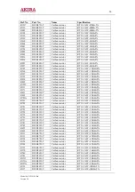
Page 49: ...W 100Ω 5 R382 D10B101J T Carbon resistor RT13 1 6W 100Ω 5 R383 D10B101J T Carbon resistor RT13 1 6W 100Ω 5 R401 D10B101J T Carbon resistor RT13 1 6W 100Ω 5 R402 D10B101J T Carbon resistor RT13 1 6W 100Ω 5 R452 D10B101J T Carbon resistor RT13 1 6W 100Ω 5 R723 D10B101J T Carbon resistor RT13 1 6W 100Ω 5 R724 D10B101J T Carbon resistor RT13 1 6W 100Ω 5 R743 D10B101J T Carbon resistor RT13 1 6W 100Ω 5...

Page 50: ...or RT13 1 6W 2 2KΩ 5 R451 D10B222J T Carbon resistor RT13 1 6W 2 2KΩ 5 R463 D10B222J T Carbon resistor RT13 1 6W 2 2KΩ 5 R701A D10B222J T Carbon resistor RT13 1 6W 2 2KΩ 5 R321 D10B272J T Carbon resistor RT13 1 6W 2 7KΩ 5 R702 D10B332J T Carbon resistor RT13 1 6W 3 3KΩ 5 R721 D10B332J T Carbon resistor RT13 1 6W 3 3KΩ 5 R722 D10B332J T Carbon resistor RT13 1 6W 3 3KΩ 5 R728 D10B332J T Carbon resis...

Page 51: ... Carbon resistor RT13 1 6W 22KΩ 5 R804 D10B223J T Carbon resistor RT13 1 6W 22KΩ 5 R1515 D10B223J T Carbon resistor RT13 1 6W 22KΩ 5 R1556 D10B223J T Carbon resistor RT13 1 6W 22KΩ 5 R484 D10B223J T Carbon resistor RT13 1 6W 27KΩ 5 R487 D10B223J T Carbon resistor RT13 1 6W 27KΩ 5 R171 D10B333J T Carbon resistor RT13 1 6W 33KΩ 5 R175 D10B333J T Carbon resistor RT13 1 6W 33KΩ 5 R317 D10B333J T Carbo...

Page 52: ...4MΩ 5 R918 Glass Glazed Fixed RES RI40 1 2W 1 5KΩ 5 R928 Glass Glazed Fixed RES RI40 1 2W 1 5KΩ 5 R938 Glass Glazed Fixed RES RI40 1 2W 1 5KΩ 5 R555 F10DR27J C Fuse resistor RF10 1 2W 0 27Ω 5 R565 F10DR27J C Fuse resistor RF10 1 2W 0 27Ω 5 R566 F10DR27J C Fuse resistor RF10 1 2W 0 27Ω 5 R165 F10DR47J C Fuse resistor RF10 1 2W 0 47Ω 5 R470 F10DR47J C Fuse resistor RF10 1 2W 0 47Ω 5 R472 F10DR47J C ...

Page 53: ...2FF103Z T Ceramic capacitor CT1 08A 2F4 50 63V 0 01uF Z C703A C2FF103Z T Ceramic capacitor CT1 08A 2F4 50 63V 0 01uF Z C723 C2FF103Z T Ceramic capacitor CT1 08A 2F4 50 63V 0 01uF Z C744 C2FF103Z T Ceramic capacitor CT1 08A 2F4 50 63V 0 01uF Z C752 C2FF103Z T Ceramic capacitor CT1 08A 2F4 50 63V 0 01uF Z C756 C2FF103Z T Ceramic capacitor CT1 08A 2F4 50 63V 0 01uF Z C482 C2BP101K T Ceramic capacitor...

Page 54: ...4 E20D101M T Electrolytic Capacitor CD110 25V 100uF M C474A E20D101M T Electrolytic Capacitor CD110 25V 100uF M C161 E20D471M Electrolytic Capacitor CD110 25V 470uF M C522 E20D102M Electrolytic Capacitor CD110 25V 1000uF M C524 E20D222M Electrolytic Capacitor CD110 25V 2200uF M C453 E20E470M T Electrolytic Capacitor CD110 35V 47uF M C530 E20E331M T Electrolytic Capacitor CD110 35V 330uF M C121 E20...

Page 55: ...11 100V 0 033uF K C1513 F20G473K T Mylar capacitor CL11 100V 0 047uF K C427 F20G473K T Mylar capacitor CL11 100V 0 047uF K C1514 F20G104K T Mylar capacitor CL11 100V 0 1uF K C460 F20G104K T Mylar capacitor CL11 100V 0 1uF K C705 F20G104K T Mylar capacitor CL11 100V 0 1uF K C706 F20G104K T Mylar capacitor CL11 100V 0 1uF K C707 F20G104K T Mylar capacitor CL11 100V 0 1uF K C467 F20J394J Polypropylen...

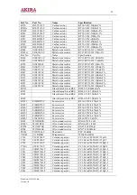
Page 56: ...018XX Diode RGP15D VD300A DZ0001XX T Diode RD5 1EB3 HZ5C1 VD481 DZ0002XX T Diode HZ22 2 VD564 DZ0006XX T Diode RD3 3L HZ3C3 VD1561 DZ0006XX T Diode RD6 4L HZ6C2 VD381 DZ0011XX T Diode RD7 1EB2 HZ7C1 VD382 DZ0011XX T Diode RD7 1EB2 HZ7C1 VD383 DZ0011XX T Diode RD7 1EB2 HZ7C1 VD1519 DZ0011XX T Diode RD7 1EB2 HZ7C1 Ref No Part No Name Specification VD460 DZ0010XX T Diode HZ9A3 VD483 DZ0010XX T Diode ...

Page 57: ...XX T Audion 2SC945 2SC1815 2SC536E V395 RXC945XX T Audion 2SC945 2SC1815 2SC536E V504 RXC945XX T Audion 2SC945 2SC1815 2SC536E V801 RXC945XX T Audion 2SC945 2SC1815 2SC536E V1553 RXC945XX T Audion 2SC945 2SC1815 2SC536E V451 RXD2140X Audion TT2190LS V701 RXC2369XX T Audion PH2369 Z352 FC0007XX Ceramic trap filter XT6 0M Z354 FC0008XX Ceramic trap filter XT5 5M Z351 FC0006XX Ceramic trap filter XT6...

Page 58: ...58 Model No 21WHS3 Bn Version 1 0 CIRCUIT DIAGRAM ...

Page 59: ......

Reviews: