background image

ASAHI KASEI 


[AKD4584] 

<KM065802>  

2009/06 


- 10 - 

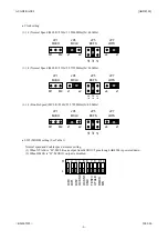
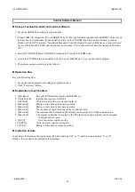
  (2) Master Mode 


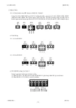
(2-1) A/D evaluation using DIT function of AK4584

Default


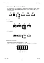
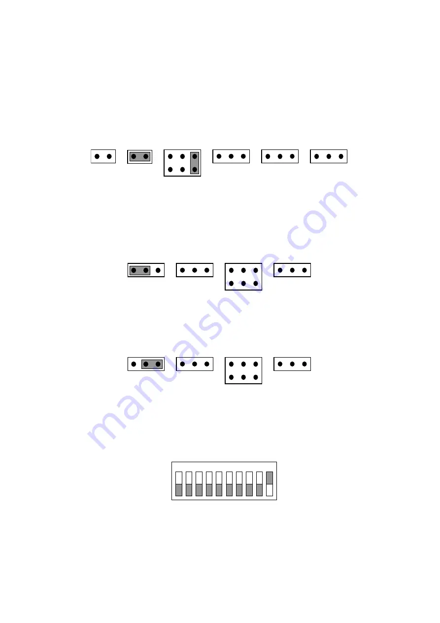
Using X’tal (X1), PORT4 (DIT) and J6 (TX). Nothing should be connected to J7 (RX), PORT1 (DIR), PORT5 

(DIR) and PORT6 (ROM). The bi-phase data is output from TX3. JP6 (EXT) should be short. In normal speed, 
double speed mode and quad speed mode, JP3 (XTI), JP4 (MCLK), JP5 (BCFS) and JP7 (LRFS) should be open. 


JP10

MCLK

JP3

XTI

JP14

LRCK

JP6

EXT

JP11

BICK

EXT

DIR

DI

R

EXT

AD

C

JP15

SDTI

ADC

DIR

EXT

DIR


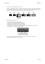
 Clock Setting 


(2-1-1) Select MCKO1 


JP5

BCFS

JP7

LRFS

JP4

MCLK

x1

x4

x4

x2

x1

JP1

MCKO

M2

M1

x2

x1


(2-1-2) Select MCKO2 


JP5

BCFS

JP7

LRFS

JP4

MCLK

x1

x4

x4

x2

x1

JP1

MCKO

M2

M1

x2

x1


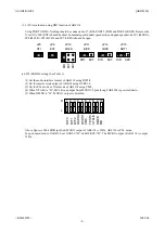
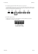
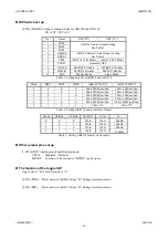
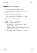
 SW2 (MODE) setting (See Table 1) 


Normal speed and double speed are same setting. 
(1)


When XTALE is “H”, MCLK can output from MCKO1/2 pins though AK4584 is powered down. 

(2)


When DMCK is “H”, MCKO1 output is disabled. 


H

L

1 2 3 4 5

8

6 7

9 10

DI

F

0

DI

F

1

DI

F

2

O

C

KS0

O

C

KS1

CM

0

TES

T

3

XT

A

L

E

DM

CK

MS


Summary of Contents for AK4584

Page 1: ...uide AKD4584 Evaluation board for AK4584 Cable for connecting with printer port of IBM AT compatible PC and control software are packed with this FUNCTION DIT DIR with optical input output BNC connector for an external clock input 10pin Header for serial control mode 10pin Header Control Data 10pin Header ROM 2 7 5 25V 4 75 5 25V GND ROUT Opt In BNC In LOUT LIN RIN BNC out Opt out AK4114 Opt In Op...

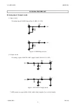
Page 2: ...N J3 LIN J1 RIN R19 560 C34 10u C32 10u RIN LIN R16 560 Figure 2 LIN RIN Input circuits 2 Output circuits The analog output of AK4584 s DAC outputs from J2 ROUT J4 LOUT ROUT C35 22u R17 10k C33 22u J2 ROUT R18 220 R20 10k J4 LOUT LOUT R15 220 Figure 3 LOUT ROUT Output circuits AKM assumes no responsibility for the trouble when using the above circuit examples ...

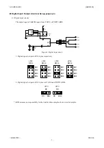
Page 3: ...7 RX RX4 PORT5 DIR 1 3 4 2 6 5 OUT VCC GND GND 6 5 RX3 C37 0 1u RX2 RX1 RX1 R40 75 Figure 4 Digital input circuit 1 Digital signal is input to RX1 4 pins respectively JP12 RX1 4 RX2 RX1 JP12 RX1 4 RX2 RX1 RX4 RX3 RX4 RX3 JP12 RX1 4 RX2 RX1 RX4 RX3 JP12 RX1 4 RX2 RX1 RX4 RX3 2 Digital signal is input to RX1 4 pins via J7 RX and PORT5 DIR JP13 RX BNC RX JP13 RX BNC RX AKM assumes no responsibility f...

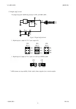
Page 4: ... R32 1k TX2 C36 0 1u R37 330 PORT4 DIT 1 2 3 4 5 6 GND IF VCC IN 5 6 Figure 5 Digital output circuit 1 Digital signal is output to TX1 3 pins respectively JP9 TX1 3 TX2 TX1 JP9 TX1 3 TX2 TX1 TX3 TX3 JP9 TX1 3 TX2 TX1 TX3 2 Digital signal is output to TX1 3 pins via J6 TX and PORT4 DIT JP8 TX BNC TX JP8 TX BNC TX AKM assumes no responsibility for the trouble when using the above circuit examples ...

Page 5: ...ase of AK4584 evaluation using AK4114 it is necessary to correspond to AK4584 s and AK4114 s audio interface format About AK4584 s audio interface format refer to AK4584 s datasheet About AK4114 s audio interface format see Table2 1 1 A D evaluation using DIT function of AK4584 1 2 A D evaluation using DIT function of AK4114 1 3 D A evaluation using DIR function of AK4114 1 4 All interfacing signa...

Page 6: ...S JP4 MCLK x1 x4 x4 x2 x1 JP1 MCKO M2 M1 x2 x1 1 1 3 Double Speed MCLK 256fs 22 5792MHz fs 88 2kHz JP5 BCFS JP7 LRFS JP4 MCLK x1 x4 x4 x2 x1 JP1 MCKO M2 M1 x2 x1 SW2 MODE setting See Table 1 Normal speed and double speed are same setting 1 When XTALE is H MCLK can output from MCKO1 2 pins though AK4584 is powered down 2 When DMCK is H MCKO1 output is disabled H L 1 2 3 4 5 8 6 7 9 10 DIF0 DIF1 DIF...

Page 7: ... JP15 SDTI ADC DIR EXT DIR SW2 MODE setting See Table 1 Normal speed and double speed are same setting 1 Set the audio interface format of AK4114 using DIF2 0 2 Set the master clock output of AK4114using OCKS1 0 3 Set the PLL mode or X tal mode of AK4114 using CM0 4 When XTALE is H MCLK can output from MCKO1 2 pins though AK4584 is powered down 5 When DMCK is H MCKO1 output is disabled H L 1 2 3 4...

Page 8: ...DTI ADC DIR EXT DIR SW2 MODE setting See Table 1 1 Set the audio interface format of AK4114 using DIF2 0 2 Set the master clock output of AK4114using OCKS1 0 3 Set the PLL mode or X tal mode of AK4114 using CM0 4 When XTALE is H MCLK can output from MCKO1 2 pins though AK4584 is powered down 5 When DMCK is H MCKO1 output is disabled H L 1 2 3 4 5 8 6 7 9 10 DIF0 DIF1 DIF2 OCKS0 OCKS1 CM0 TEST3 XTA...

Page 9: ...ort In normal speed double speed mode and quad speed mode JP1 MCKO JP4 MCLK JP5 BCFS and JP7 LRFS should be open JP10 MCLK JP3 XTI JP14 LRCK JP6 EXT JP11 BICK EXT DIR DIR EXT ADC JP15 SDTI ADC DIR EXT DIR SW2 MODE setting See Table 1 1 When XTALE is H MCLK can output from MCKO1 2 pins though AK4584 is powered down 2 When DMCK is H MCKO1 output is disabled H L 1 2 3 4 5 8 6 7 9 10 DIF0 DIF1 DIF2 OC...

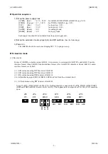
Page 10: ... LRFS should be open JP10 MCLK JP3 XTI JP14 LRCK JP6 EXT JP11 BICK EXT DIR DIR EXT ADC JP15 SDTI ADC DIR EXT DIR Clock Setting 2 1 1 Select MCKO1 JP5 BCFS JP7 LRFS JP4 MCLK x1 x4 x4 x2 x1 JP1 MCKO M2 M1 x2 x1 2 1 2 Select MCKO2 JP5 BCFS JP7 LRFS JP4 MCLK x1 x4 x4 x2 x1 JP1 MCKO M2 M1 x2 x1 SW2 MODE setting See Table 1 Normal speed and double speed are same setting 1 When XTALE is H MCLK can output...

Page 11: ...XT JP11 BICK EXT DIR DIR EXT ADC JP15 SDTI ADC DIR EXT DIR Clock setting 2 2 1 Select MCKO1 JP5 BCFS JP7 LRFS JP4 MCLK x1 x4 x4 x2 x1 JP1 MCKO M2 M1 x2 x1 2 2 2 Select MCKO2 JP5 BCFS JP7 LRFS JP4 MCLK x1 x4 x4 x2 x1 JP1 MCKO M2 M1 x2 x1 SW2 MODE setting See Table 1 Normal speed double speed and quad speed mode are same setting 1 When XTALE is H MCLK can output from MCKO1 2 pins though AK4584 is po...

Page 12: ...tified 1 0 0 1 24bit MSB justified 18bit LSB justified 2 0 1 0 24bit MSB justified 20bit LSB justified 3 0 1 1 24bit MSB justified 24bit LSB justified 4 1 0 0 24bit MSB justified 24bit MSB justified 5 1 0 1 24bit I2 S 24bit I2 S Table 2 Setting AK4114 audio interface format Mode OCKS1 OCKS0 MCKO1 X tal fs 0 0 0 256fs 256fs 96kHz 1 0 1 256fs 256fs 96kHz 2 1 0 512fs 512fs 48kHz 3 1 1 128fs 128fs 192...

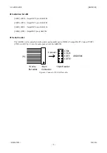
Page 13: ...T0 pin of AK4114 LED4 DZF Output DZF pin of AK4584 Serial Control The AK4584 can be controlled via the printer port parallel port of IBM AT compatible PC Connect PORT3 CTRL with PC by 10 wire flat cable packed with the AKD4584 Connect CSN CCLK CDTI 10pin Header 10pin Connector 10 wire flat cable PC AKD4584 CDTO Figure 6 Connect of 10 wire flat cable ...

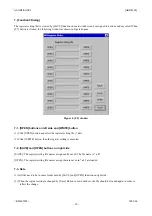
Page 14: ...on flow Keep the following flow 1 Set up the control program according to explanation above 2 Click Port Reset button Explanation of each buttons 1 Port Reset Set up the USB interface board AKDUSBIF A 2 Write default Initialize the register of AK4584 3 All Write Write all registers that is currently displayed 4 Function1 Dialog to write data by keyboard operation 5 Function2 Dialog to write data b...

Page 15: ... click Cancel button 3 Function2 Dialog Dialog to evaluate GAIN ATT This dialog corresponds to address 04H 05H 06H and 07H Address Box Input registers address in 2 figures of hexadecimal Start Data Box Input starts data in 2 figures of hexadecimal End Data Box Input end data in 2 figures of hexadecimal Interval Box Data is written to AK4584 by this interval Step Box Data changes by this step Mode ...

Page 16: ...ion of file name is akr Operation flow 1 Click Save Button 2 Set the file name and push Save Button The extension of file name is akr 4 2 Open The register setting data saved by Save is written to AK4584 The file type is the same as Save Operation flow 1 Click Open Button 2 Select the file akr and Click Open Button ...

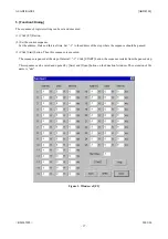
Page 17: ...Interval time Set 1 to the address of the step where the sequence should be paused 3 Click Start button Then this sequence is executed The sequence is paused at the step of Interval 1 Click START button the sequence restarts from the paused step This sequence can be saved and opened by Save and Open button on the Function3 window The extension of file name is aks Figure 1 Window of F3 ...

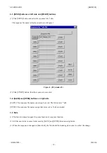
Page 18: ... AKD4584 KM065802 2009 06 18 6 Function4 Dialog The sequence that is created on Function3 can be assigned to buttons and executed When F4 button is clicked the window as shown in Figure 2 opens Figure 2 F4 window ...

Page 19: ...s executed 3 2 SAVE and OPEN buttons on right side SAVE The sequence file names can assign be saved The file name is ak4 OPEN The sequence file names assign that are saved in ak4 are loaded 3 3 Note 1 This function doesn t support the pause function of sequence function 2 All files need to be in same folder used by SAVE and OPEN function on right side 3 When the sequence is changed in Function3 th...

Page 20: ...tton and select the register setting file akr 2 Click WRITE button then the register setting is executed 7 2 SAVE and OPEN buttons on right side SAVE The register setting file names assign can be saved The file name is ak5 OPEN The register setting file names assign that are saved in ak5 are loaded 7 3 Note 1 All files need to be in same folder used by SAVE and OPEN function on right side 2 When t...

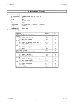
Page 21: ...it ADC Analog Input Characteristics S N D fs 44 1kHz 0 5dB Input fs 96kHz 0 5dB Input 92 0 88 3 dB dB D Range fs 44 1kHz 60dB Input A weighted fs 96kHz 60dB Input 100 6 96 1 dB dB S N fs 44 1kHz A weighted fs 96kHz 101 0 96 1 dB dB Interchannel Isolation 110 5 dB DAC Analog Output Characteristics S N D fs 44 1kHz 0dB Output fs 96kHz 0 5dB Output 95 3 95 1 dB dB D Range fs 44 1kHz 60dB Output A wei...

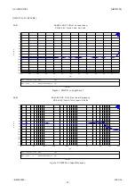
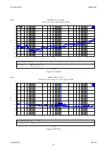
Page 22: ...108 106 104 102 100 98 96 94 92 90 88 86 84 82 d B F S 120 10 110 100 90 80 70 60 50 40 30 20 dBr Figure 1 THD N vs Input Level AKM AK4584 ADC THD N vs Input Frequency VDD 5 0V fs 44 1kHz Input 0 5dBr last at2c Color Line Style Thick Data Axis Blue Solid 3 DSP Anlr THD N Am pl A Left 110 80 108 106 104 102 100 98 96 94 92 90 88 86 84 82 d B F S 20 20k 50 100 200 500 1k 2k 5k 10k Hz Figure 2 THD N ...

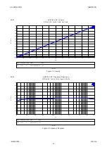
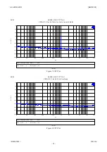
Page 23: ...ft 120 0 110 100 90 80 70 60 50 40 30 20 10 d B F S 120 0 110 100 90 80 70 60 50 40 30 20 10 dBr Figure 3 Linearity AKM AK4584 ADC Frequency Response VDD 5 0V fs 44 1kHz Input 0 5dBr last at2c Color Line Style Thick Data Axis Blue Solid 3 DSP Anlr Am pl A Left 1 0 0 9 0 8 0 7 0 6 0 5 0 4 0 3 0 2 0 1 d B F S 20 20k 50 100 200 500 1k 2k 5k 10k Hz Figure 4 Frequency Response ...

Page 24: ...e Solid 3 DSP Anlr Cross talk A Left 140 80 135 130 125 120 115 110 105 100 95 90 85 d B 20 20k 50 100 200 500 1k 2k 5k 10k Hz Figure 5 Crosstalk AKM AK4584 ADC FFT Plot VDD 5 0V fs 44 1kHz fin 1kHz Input 0 5dBr last at2c Color Line Style Thick Data Axis Blue Solid 3 Fft Ch 1 Am pl Left 180 0 160 140 120 100 80 60 40 20 d B F S 20 20k 50 100 200 500 1k 2k 5k 10k Hz Figure 6 FFT Plot ...

Page 25: ... Solid 3 Fft Ch 1 Am pl Left 180 0 160 140 120 100 80 60 40 20 d B F S 20 20k 50 100 200 500 1k 2k 5k 10k Hz Figure 7 FFT Plot AKM AK4584 ADC FFT Plot VDD 5 0V fs 44 1kHz fin None last at2c Color Line Style Thick Data Axis Blue Solid 3 Fft Ch 1 Am pl Left 180 0 160 140 120 100 80 60 40 20 d B F S 20 20k 50 100 200 500 1k 2k 5k 10k Hz Figure 8 FFT Plot ...

Page 26: ...100 90 80 70 60 50 40 30 20 dBr 110 80 108 106 104 102 100 98 96 94 92 90 88 86 84 82 d B F S Figure 9 THD N vs Input Level AKM AK4584 ADC THD N vs Input Frequency VDD 5 0V fs 96kHz Input 0 5dBr last at2c Color Line Style Thick Data Axis Blue Solid 3 DSP Anlr THD N Am pl A Left 20 40k 50 100 200 500 1k 2k 5k 10k 20k Hz 110 80 108 106 104 102 100 98 96 94 92 90 88 86 84 82 d B F S Figure 10 THD N v...

Page 27: ...120 0 110 100 90 80 70 60 50 40 30 20 10 dBr 120 0 110 100 90 80 70 60 50 40 30 20 10 d B F S Figure 11 Linearity AKM AK4584 ADC Frequency Response VDD 5 0V fs 96kHz Input 0 5dBr last at2c Color Line Style Thick Data Axis Blue Solid 3 DSP Anlr Am pl A Left 20 40k 50 100 200 500 1k 2k 5k 10k 20k Hz 1 0 0 9 0 8 0 7 0 6 0 5 0 4 0 3 0 2 0 1 d B F S Figure 12 Frequency Response ...

Page 28: ...id 3 DSP Anlr Cross talk A Left 20 40k 50 100 200 500 1k 2k 5k 10k 20k Hz 140 80 135 130 125 120 115 110 105 100 95 90 85 d B Figure 13 Crosstalk AKM AK4584 ADC FFT Plot VDD 5 0V fs 96kHz fin 1kHz Input 0 5dBr last at2c Color Line Style Thick Data Axis Blue Solid 3 Fft Ch 1 Am pl Left 180 0 160 140 120 100 80 60 40 20 d B F S 20 40k 50 100 200 500 1k 2k 5k 10k 20k Hz Figure 14 FFT Plot ...

Page 29: ...d 3 Fft Ch 1 Am pl Left 180 0 160 140 120 100 80 60 40 20 d B F S 20 40k 50 100 200 500 1k 2k 5k 10k 20k Hz Figure 15 FFT Plot AKM AK4584 ADC FFT Plot VDD 5 0V fs 96kHz fin None last at2c Color Line Style Thick Data Axis Blue Solid 3 Fft Ch 1 Am pl Left 180 0 160 140 120 100 80 60 40 20 d B F S 20 40k 50 100 200 500 1k 2k 5k 10k 20k Hz Figure 16 FFT Plot ...

Page 30: ...08 106 104 102 100 98 96 94 92 90 88 86 84 82 d B r A 120 0 110 100 90 80 70 60 50 40 30 20 10 dBFS Figure 1 THD N vs Input Level AKM AK4584 DAC THD N vs Input Frequency VDD 5 0V fs 44 1kHz Input 0dBFS last at2c Color Line Style Thick Data Axis Blue Solid 3 Anlr THD N Am pl Left 110 80 108 106 104 102 100 98 96 94 92 90 88 86 84 82 d B r A 20 20k 50 100 200 500 1k 2k 5k 10k Hz Figure 2 THD N vs In...

Page 31: ...eft 120 0 110 100 90 80 70 60 50 40 30 20 10 d B r A 120 0 110 100 90 80 70 60 50 40 30 20 10 dBFS Figure 3 Linearity AKM AK4584 DAC Frequency Response VDD 5 0V fs 44 1kHz Input 0dBFS last at2c Color Line Style Thick Data Axis Blue Solid 3 Anlr Am pl Left 1 1 0 8 0 6 0 4 0 2 0 0 2 0 4 0 6 0 8 d B r A 2k 20k 4k 6k 8k 10k 12k 14k 16k 18k Hz Figure 4 Frequency Response ...

Page 32: ...3 Anlr Cros stalk Left 130 100 127 5 125 122 5 120 117 5 115 112 5 110 107 5 105 102 5 d B 20 20k 50 100 200 500 1k 2k 5k 10k Hz Figure 5 Crosstalk AKM AK4584 DAC FFT Plot VDD 5 0V fs 44 1kHz fin 1kHz Input 0dBFS last at2c Color Line Style Thick Data Axis Blue Solid 3 Fft Ch 1 Am pl Left 180 0 160 140 120 100 80 60 40 20 d B r A 20 20k 50 100 200 500 1k 2k 5k 10k Hz Figure 6 FFT Plot ...

Page 33: ...e Solid 3 Fft Ch 1 Am pl Left 180 0 160 140 120 100 80 60 40 20 d B r A 20 20k 50 100 200 500 1k 2k 5k 10k Hz Figure 7 FFT Plot AKM AK4584 DAC FFT Plot VDD 5 0V fs 44 1kHz fin None last at2c Color Line Style Thick Data Axis Blue Solid 3 Fft Ch 1 Am pl Left 180 0 160 140 120 100 80 60 40 20 d B r A 20 20k 50 100 200 500 1k 2k 5k 10k Hz Figure 8 FFT Plot ...

Page 34: ...06 104 102 100 98 96 94 92 90 88 86 84 82 d B r A 120 0 110 100 90 80 70 60 50 40 30 20 10 dBFS Figure 9 THD N vs Input Level AKM AK4584 DAC THD N vs Input Frequency VDD 5 0V fs 96kHz Input 0dBFS last at2c Color Line Style Thick Data Axis Blue Solid 3 Anlr THD N Am pl Left 110 80 108 106 104 102 100 98 96 94 92 90 88 86 84 82 d B r A 20 40k 50 100 200 500 1k 2k 5k 10k 20k Hz Figure 10 THD N vs Inp...

Page 35: ... 90 80 70 60 50 40 30 20 10 d B r A 120 0 110 100 90 80 70 60 50 40 30 20 10 dBFS Figure 11 Linearity AKM AK4584 DAC Frequency Response VDD 5 0V fs 96kHz Input 0dBFS last at2c Color Line Style Thick Data Axis Blue Solid 3 Anlr Am pl Left 1 1 0 8 0 6 0 4 0 2 0 0 2 0 4 0 6 0 8 d B r A 2 5k 40k 5k 7 5k 10k 12 5k 15k 17 5k 20k 22 5k 25k 27 5k 30k 32 5k 35k 37 5k Hz Figure 12 Frequency Response ...

Page 36: ...lue Solid 3 Anlr Cros stalk Left 130 90 125 120 115 110 105 100 95 d B 20 40k 50 100 200 500 1k 2k 5k 10k 20k Hz Figure 13 Crosstalk AKM AK4584 DAC FFT Plot VDD 5 0V fs 96kHz fin 1kHz Input 0dBFS last at2c Color Line Style Thick Data Axis Blue Solid 3 Fft Ch 1 Am pl Left 180 0 160 140 120 100 80 60 40 20 d B r A 20 40k 50 100 200 500 1k 2k 5k 10k 20k Hz Figure 14 FFT Plot ...

Page 37: ...id 3 Fft Ch 1 Am pl Left 180 0 160 140 120 100 80 60 40 20 d B r A 20 40k 50 100 200 500 1k 2k 5k 10k 20k Hz Figure 15 FFT Plot AKM AK4584 DAC FFT Plot VDD 5 0V fs 96kHz fin None last at2c Color Line Style Thick Data Axis Blue Solid 3 Fft Ch 1 Am pl Left 180 0 160 140 120 100 80 60 40 20 d B r A 20 40k 50 100 200 500 1k 2k 5k 10k 20k Hz Figure 16 FFT Plot ...

Page 38: ...t 180 0 160 140 120 100 80 60 40 20 d B r A 20 40k 50 100 200 500 1k 2k 5k 10k 20k Hz Figure 17 Outband Noise fs 44 1kHz AKM AK4584 DAC FFT Plot VDD 5 0V fs 96kHz fin None last at2c Color Line Style Thick Data Axis Blue Solid 3 Fft Ch 1 Am pl Left 180 0 160 140 120 100 80 60 40 20 d B r A 20 80k 50 100 200 500 1k 2k 5k 10k 20k 50k Hz Figure 18 Outband Noise fs 96kHz ...

Page 39: ...designed or intended for life support or maintenance of safety or for applications in medicine aerospace nuclear energy or other fields in which its failure to function or perform may reasonably be expected to result in loss of life or in significant injury or damage to person or property b A critical component is one whose failure to function or perform may reasonably be expected to result whethe...

Page 40: ...C1 47u 1 2 R3 10k RP1 47k 6 5 4 3 2 1 R1 5 1 JP1 MCKO U1A 74HC14 1 2 JP2 GND C2 10u 1 2 R2 5 1 U3A 74HCT04 1 2 R5 100 JP3 XTI CN1 34 35 36 37 38 39 40 41 42 43 44 C14 47u 1 2 C10 0 1u U3B 74HCT04 3 4 D1 HSU119 2 1 CN2 1 2 3 4 5 6 7 8 9 10 11 C13 10u 1 2 C8 2 2u 1 2 C12 10u 1 2 C6 0 1u R7 100 C5 0 1u LED1 INT0 2 1 RP2 47k 6 5 4 3 2 1 CN4 12 13 14 15 16 17 18 19 20 21 22 CN3 23 24 25 26 27 28 29 30 ...

Page 41: ...GND PORT1 DIR 1 3 4 2 6 5 OUT VCC GND GND 6 5 PORT2 DIT 1 2 3 4 5 6 GND IF VCC IN 5 6 C29 10u R13 51 C26 5p C22 0 1u C27 0 1u C28 0 1u R14 1k C21 10u LED3 ERF 2 1 C19 0 1u RP3 47k 1 2 3 4 5 6 7 8 9 10 11 C25 0 1u X2 11 2896MHz 1 2 U1D 74HC14 9 8 C24 5p R9 470 SW3 DIR 2 1 3 C31 0 1u U5 AK4114 1 2 3 4 5 6 7 8 9 10 11 13 14 15 16 17 18 19 20 21 22 23 26 27 28 29 30 31 32 33 34 35 36 38 39 40 41 42 43...

Page 42: ...er Rev Date Sheet of RIN LIN ROUT DZF LOUT VCC AVDD J1 RIN U1F 74HC14 13 12 C34 10u R17 10k J3 LIN R19 560 R16 560 U3D 74HCT04 9 8 U3F 74HCT04 13 12 J4 LOUT LED4 DZF 2 1 C35 22u C33 22u U3E 74HCT04 11 10 U1E 74HC14 11 10 R21 1k C32 10u TR1 RN1202 1 3 2 J2 ROUT R18 220 R15 220 R20 10k U6A 74AC74 2 5 3 6 4 1 D Q CLK Q PR CL ...

Page 43: ...A2 A3 A4 A5 A6 A7 A8 G1 G2 Y1 Y2 Y3 Y4 Y5 Y6 Y7 Y8 C42 0 1u J7 RX C36 0 1u PORT4 DIT 1 2 3 4 5 6 GND IF VCC IN 5 6 U8 74HC4040 10 11 9 7 6 5 3 2 4 13 12 14 15 1 CLK RST Q1 Q2 Q3 Q4 Q5 Q6 Q7 Q8 Q9 Q10 Q11 Q12 JP9 TX1 3 JP13 RX JP8 TX C44 0 1u JP6 EXT R25 470 JP5 BCFS JP10 MCLK C43 0 1u R23 470 C47 0 1u R24 100 U6B 74AC74 12 9 11 8 10 13 D Q CLK Q PR CL R41 10k R33 51 C41 0 1u R26 100 C48 47u T2 DA ...

Page 44: ......

Page 45: ......

Page 46: ......

Reviews: