background image

ALINX Xilinx Core Board AC6150 User Manual

12 / 21

Amazon Store: https://www.amazon.com/alinx

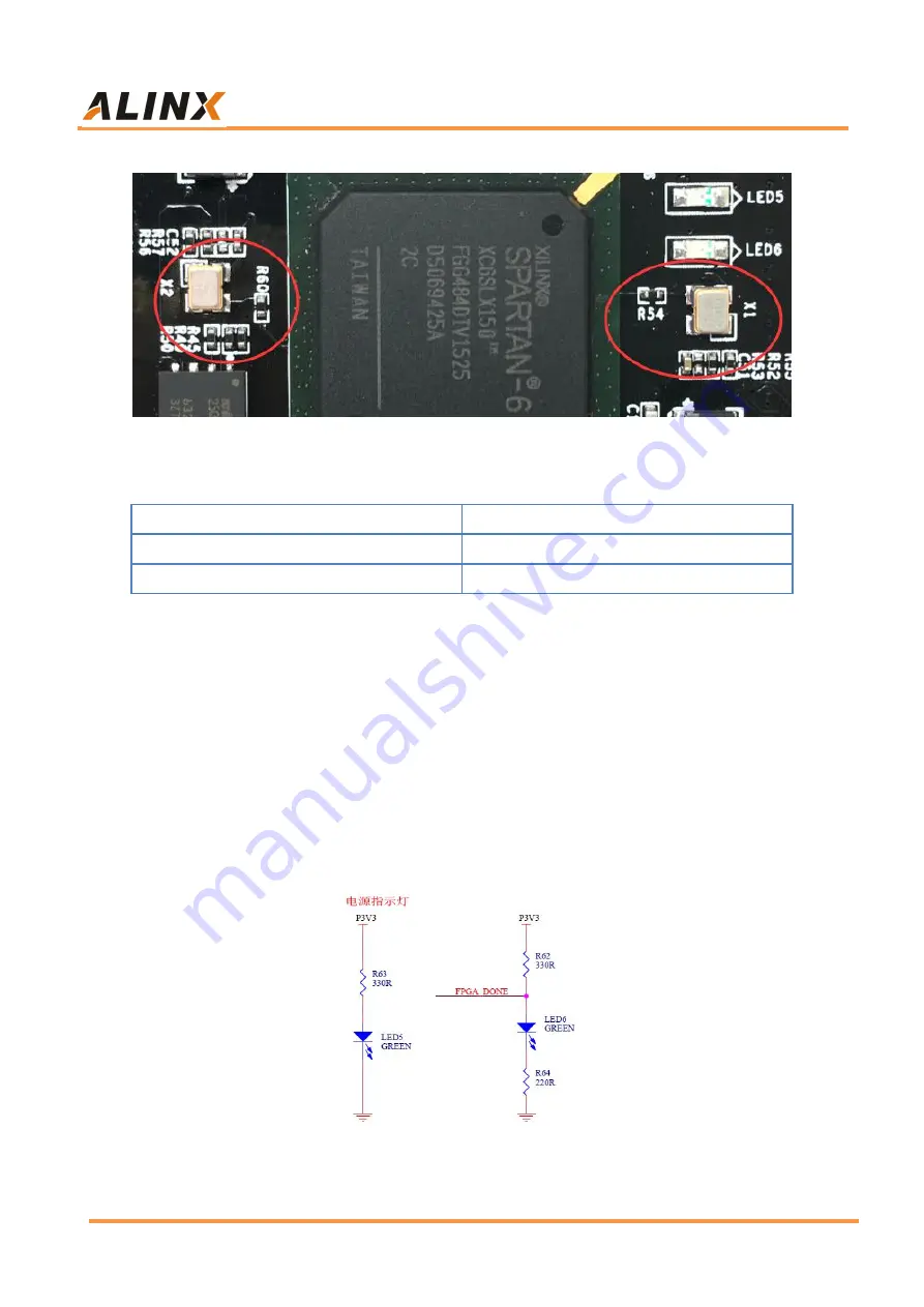
Figure 5-2: Crystal oscillator on the Core Board

Crystal oscillator Pin Assignment

Input Clock

FPGA Pin

50MHz

AB13

27MHz

B10

Part 6: LED Light on Core Board

There are 6 red LED lights on the AC6045 FPGA core board, one of which

is the power indicator light (PWR), one is the configuration LED light (DONE),
and four are the user LED light. When the core board is powered, the power
indicator will illuminate; when the FPGA is configured, the configuration LED
will illuminate.

Figure 6-1: Power Indicator and Configure Indicator schemtaic

Summary of Contents for AC6150

Page 1: ...Xilinx ALINX Core Board AC6150 User Manual ...

Page 2: ...ALINX Xilinx Core Board AC6150 User Manual 2 21 Amazon Store https www amazon com alinx Version Record Version Date Release By Description Rev 1 0 2020 11 08 Rachel Zhou First Release ...

Page 3: ...Record 2 Part 1 AC6150 core board 4 Part 2 FPGA 5 Part 2 1 JTAG Interface 6 Part 3 DDR3 DRAM 7 Part 4 SPI Flash 9 Part 5 Crystal oscillator on Core Board 11 Part 6 LED Light on Core Board 12 Part 7 AC6150 Power Supply 14 Part 8 Power interface on Core Board 16 Part 9 Expansion Ports 17 Part 10 Structure Diagram 21 ...

Page 4: ...isition This core board uses MICRON s MT41J128M16LA 187E DDR3 chip with a capacity of 2Gbit 16bit bus mode read and write data bandwidth between FPGA and DDR3 is up to 10Gb this configuration can meet the needs of 4 channels of 1080p video processing This core board also extends 168 IO ports 84 pairs of LVDS differential pairs which is a good choice for users who need a lot of IO Moreover the FPGA...

Page 5: ...tioned above the FPGA model we use is XC6SLX150 2FG484C which belongs to Xilinx s SPARTAN6 series The speed grade is 2 and the temperature grade is Commercial grade This model is a FGG484 package with 484 pins Xilinx SPARTAN6 FPGA naming rules as below Figure 2 1 The Specific Chip Model Definition of SPARTAN6 Series ...

Page 6: ...ells 147 443 Slices 23038 CLB flip flops 184 304 Block RAM kb 4 824 Clock Management Unit CMT 6 DSP Processing Unit DSP48A1 Slices 180 DDR Controller Memory Controller Blocks 4 Chip Package BGA484 Spacing 1 0mm Speed Grade 2 Temperature Grade Commercial Part 2 1 JTAG Interface First introduce the configuration and debugging interface of the FPGA JTAG interface JTAG test holes 2 5mm single row inte...

Page 7: ...core JTAG ports with DuPont cable To achieve core board program download and debug of the FPGA chip without the carrier board The following Figure 3 2 3 shows the JTAG interface on the core board Figure 2 3 JTAG Interface on the core board Part 3 DDR3 DRAM Figure 3 1 detailed part of the DDR3 schematic For details please refer to the schematic provided by us Figure 3 1 DDR3 schematic ...

Page 8: ...mal operation of DDR3 requires DDR3 address line and control line to provide termination voltage VTT and DDR3 chip reference voltage VREF VTT and VREF voltage are both 0 75V the following Figure 3 2 is the power part schematic Figure 3 2 DDR3 Power for VTT VREF Figure 3 3 DDR3 Power Circuit on the FPGA Board ...

Page 9: ...CAS K4 DDR3_A 8 E3 DDR3_CKE D2 DDR3_A 9 E1 DDR3_CLK_P H4 DDR3_A 10 G4 DDR3_CLK_N H3 DDR3_nRAS K5 DDR3_DQ 8 P2 DDR3_nWE F2 DDR3_DQ 9 P1 DDR3_ODT J6 DDR3_DQ 10 R3 DDR3_RESET C3 DDR3_DQ 11 R1 DDR3_LDM L4 DDR3_DQ 12 U3 DDR3_UDM M3 DDR3_DQ 13 U1 DDR3_DQ 0 N3 DDR3_DQ 14 V2 DDR3_DQ 1 N1 DDR3_DQ 15 V1 DDR3_DQ 2 M2 DDR3_LDQS_P L3 DDR3_DQ 3 M1 DDR3_LDQS_N L1 DDR3_DQ 4 J3 DDR3_UDQS_P T2 DDR3_DQ 5 J1 DDR3_UDQ...

Page 10: ...em to store the boot image of the system These images mainly include FPGA bit files core application code and other user data files The specific models and related parameters of SPI FLASH are shown in Table 4 1 Position Model Capacity Factory U8 W25Q64BV 64M Bit Winbond Table 4 1 SPI FLASH Specification Figure 4 1 SPI Flash schematic Figure 4 2 W25Q64BV chip on the FPGA Board ...

Page 11: ...PI_CLK Y21 SPI_CSn T5 SPI_DIN AB20 SPI_DOUT AA20 Part 5 Crystal oscillator on Core Board The core board carries a 50M active crystal oscillator and a 27M active crystal oscillator The 50MHz clock is connected to the AB13 pin of the FPGA and the 27MHz clock is connected to the B10 pin of the FPGA Figure 5 1 Crystal oscillator Schematic ...

Page 12: ...MHz B10 Part 6 LED Light on Core Board There are 6 red LED lights on the AC6045 FPGA core board one of which is the power indicator light PWR one is the configuration LED light DONE and four are the user LED light When the core board is powered the power indicator will illuminate when the FPGA is configured the configuration LED will illuminate Figure 6 1 Power Indicator and Configure Indicator sc...

Page 13: ...om alinx Figure 6 2 Power Indicator and Configure Indicator on the Core Board The schematic diagram of the four user LED sections is shown below In Figure 6 3 When the FPGA pin output is logic 0 the LED will be lit Figure 6 3 User LED Schematic Figure 6 4 User LED on the Core Board ...

Page 14: ... here The VCCO of the FPGA is separated from the VCCAUX power supply The purpose is to enable the BANK IO voltage of the FPGA to be flexibly adjusted Different output voltages are obtained by adjusting the resistance value of the VCCIO power supply section so that the IO level of the FPGA core board can be applied to different voltages The three way power supply P1V2 VCCIO P1V5 adopts the TLV62130...

Page 15: ...ALINX Xilinx Core Board AC6150 User Manual 15 21 Amazon Store https www amazon com alinx Figure 7 1 Power Supply on core board schematic ...

Page 16: ...the FPGA expansion baord needs to provide a 5V power supply to the core board through the expansion ports The power supply voltage of the core board ranges from 4 5V to 5 5V and the current is about 1A In order to ensure a certain margin the FPGA carrier boardIt is best to provide 5V 2A current The FPGA carrier boardprovide the 5V power input to the core board through pin 1 to 4 of the expansion p...

Page 17: ... board Otherwise current conflict may occur and the USB interface of the computer may be burned out Figure 8 2 Mini USB on the Core Board Part 9 Expansion Ports The core board has a total of two high speed expansion ports which is connected with the FPGA carrier board by two 100 pin inter board connectors The inter board connector uses AMP Tyco board to board connector 5177984 4 with a PIN pitch o...

Page 18: ...ALINX Xilinx Core Board AC6150 User Manual 18 21 Amazon Store https www amazon com alinx Figure 9 1 Expansion Ports P1 ...

Page 19: ...ALINX Xilinx Core Board AC6150 User Manual 19 21 Amazon Store https www amazon com alinx Figure 9 2 Expansion Ports P2 ...

Page 20: ...ALINX Xilinx Core Board AC6150 User Manual 20 21 Amazon Store https www amazon com alinx Figure 9 3 Expansion Ports P1 P2 on the Core Board ...

Page 21: ...LINX Xilinx Core Board AC6150 User Manual 21 21 Amazon Store https www amazon com alinx Part 10 Structure Diagram Figure 10 1 AC6150 FPGA Core board Top view Figure 10 2 AC6150 FPGA Core board Rear view ...

Reviews: