background image

ZYNQ Ultr FPGA Board AXU2CGA/B User Manual

11 / 29

Amazon Store: https://www.amazon.com/alinx

PS_DDR4_DQ56

PS_DDR_DQ56_504

J28

PS_DDR4_DQ57

PS_DDR_DQ57_504

K27

PS_DDR4_DQ58

PS_DDR_DQ58_504

H28

PS_DDR4_DQ59

PS_DDR_DQ59_504

H27

PS_DDR4_DQ60

PS_DDR_DQ60_504

G26

PS_DDR4_DQ61

PS_DDR_DQ61_504

G25

PS_DDR4_DQ62

PS_DDR_DQ62_504

K25

PS_DDR4_DQ63

PS_DDR_DQ63_504

J25

PS_DDR4_DM4

PS_DDR_DM4_504

R23

PS_DDR4_DM5

PS_DDR_DM5_504

H23

PS_DDR4_DM6

PS_DDR_DM6_504

L27

PS_DDR4_DM7

PS_DDR_DM7_504

H26

Part 4: QSPI Flash

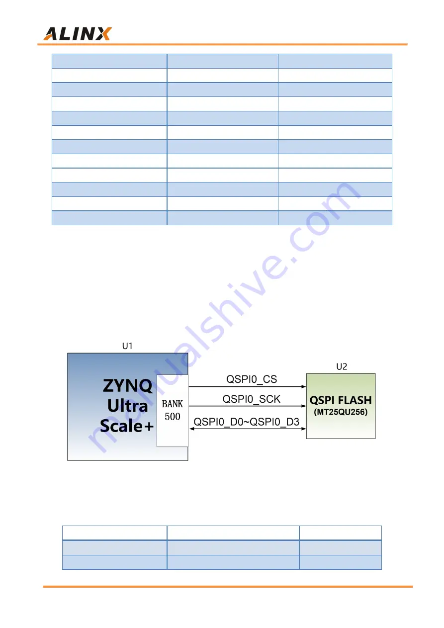
The AXU2CGA/B board has a 256MBit Quad-SPI FLASH chip, the model

is MT25QU256ABA1EW9-0SIT. QSPI FLASH is connected to the GPIO port of
BANK500 in the PS part of the ZYNQ chip. Figure 4-1 shows the part of QSPI
Flash in the schematic.

Figure 4-1: QSPI Flash

Configure Chip Pin Assignment:

Signal Name

Pin Name

Pin Number

MIO0_QSPI0_SCLK

PS_MIO0_500

AG15

MIO1_QSPI0_IO1

PS_MIO1_500

AG16

Summary of Contents for AXU2CGA

Page 1: ...ZYNQ UltraScale FPGA Development Board AXU2CGA B User Manual ...

Page 2: ...ZYNQ Ultrascale FPGA Board AXU2CGA B User Manual 2 29 Amazon Store https www amazon com alinx Version Record Version Date Release By Description Rev 1 0 2021 04 08 Rachel Zhou First Release ...

Page 3: ...6 EEPROM 13 Part 7 DP Display Interface 13 Part 8 USB 3 0 Interface 15 Part 9 Gigabit Ethernet Interface 16 Part 10 USB to Serial Port 17 Part 11 SD Card Slot Interface 18 Part 12 PCIE Interface 19 Part 13 40 Pin Expansion Header 20 Part 14 MIPI Camera Interface 22 Part 15 JTAG Debug Port 24 Part 16 DIP Switch Configuration 25 Part 17 LEDs 25 Part 18 System Clock 26 Part 19 ALINX Customized Fan In...

Page 4: ...4E The PS side of AXU2CGA is mounted with 2 slices of DDR4 total 1GB 32bit and 1 slice of 256Mb QSPI FLASH The PS side of AXU2CGB is equipped with 4 DDR4 total 2GB 64bit one 8GB eMMC FLASH memory chip and one 256Mb QSPI FLASH Peripheral interfaces include 1 MINI DP interface 4 USB3 0 interfaces 1 Gigabit Ethernet interface 1 USB serial port 1 PCIE interface 1 TF card interface 2 40 pin expansion p...

Page 5: ... with a speed of up to 500Mhz The XCZU2CG Chip supports 32 bit or 64 bit DDR4 LPDDR4 DDR3 DDR3L LPDDR3 memory chips with rich high speed interfaces on the PS side such as PCIE Gen2 USB3 0 SATA 3 1 DisplayPort it also supports USB2 0 Gigabit Ethernet SD SDIO I2C CAN UART GPIO and other interfaces The PL end contains a wealth of programmable logic units DSP and internal RAM The overall block diagram...

Page 6: ...L LPDDR4 3 interface Static storage interface support NAND 2xQuad SPI FLASH High speed connection interface support PCIe Gen2 x4 2xUSB3 0 Sata 3 1 Display Port 4 x Tri mode Gigabit Ethernet Common connection interface 2xUSB2 0 2x SD SDIO 2x UART 2x CAN 2 0B 2x I2C 2x SPI 4x 32b GPIO Power management support the division of Full Low PL Battery four parts of power Encryption algorithm support RSA AE...

Page 7: ...d of DDR4 SDRAM on the PS side can reach 1200MHz data rate 2400Mbps The specific configuration of DDR4 SDRAM is shown below Among them U71 and U72 are only AXU2CGB mounted Location Capacity Manufacturer U3 U5 U71 U72 256M x 16bit Micron Table 3 1 DDR4 SDRAM Configuration The hardware connection of DDR4 on the PS side is shown in Figure 3 1 Figure 3 1 PS Side DDR4 DRAM Schematic AXU2CGA PS side DDR...

Page 8: ..._504 AH22 PS_DDR4_DQ10 PS_DDR_DQ10_504 AE22 PS_DDR4_DQ11 PS_DDR_DQ11_504 AD22 PS_DDR4_DQ12 PS_DDR_DQ12_504 AH23 PS_DDR4_DQ13 PS_DDR_DQ13_504 AH24 PS_DDR4_DQ14 PS_DDR_DQ14_504 AE24 PS_DDR4_DQ15 PS_DDR_DQ15_504 AG24 PS_DDR4_DQ16 PS_DDR_DQ16_504 AC26 PS_DDR4_DQ17 PS_DDR_DQ17_504 AD26 PS_DDR4_DQ18 PS_DDR_DQ18_504 AD25 PS_DDR4_DQ19 PS_DDR_DQ19_504 AD24 PS_DDR4_DQ20 PS_DDR_DQ20_504 AG26 PS_DDR4_DQ21 PS_...

Page 9: ...504 AA22 PS_DDR4_A9 PS_DDR_A9_504 AB23 PS_DDR4_A10 PS_DDR_A10_504 AA25 PS_DDR4_A11 PS_DDR_A11_504 AA26 PS_DDR4_A12 PS_DDR_A12_504 AB25 PS_DDR4_A13 PS_DDR_A13_504 AB26 PS_DDR4_WE_B PS_DDR_A14_504 AB24 PS_DDR4_CAS_B PS_DDR_A15_504 AC24 PS_DDR4_RAS_B PS_DDR_A16_504 AC23 PS_DDR4_ACT_B PS_DDR_ACT_N_504 Y23 PS_DDR4_ALERT_B PS_DDR_ALERT_N_504 U25 PS_DDR4_BA0 PS_DDR_BA0_504 V23 PS_DDR4_BA1 PS_DDR_BA1_504 ...

Page 10: ..._504 T22 PS_DDR4_DQ33 PS_DDR_DQ33_504 R22 PS_DDR4_DQ34 PS_DDR_DQ34_504 P22 PS_DDR4_DQ35 PS_DDR_DQ35_504 N22 PS_DDR4_DQ36 PS_DDR_DQ36_504 T23 PS_DDR4_DQ37 PS_DDR_DQ37_504 P24 PS_DDR4_DQ38 PS_DDR_DQ38_504 R24 PS_DDR4_DQ39 PS_DDR_DQ39_504 N24 PS_DDR4_DQ40 PS_DDR_DQ40_504 H24 PS_DDR4_DQ41 PS_DDR_DQ41_504 J24 PS_DDR4_DQ42 PS_DDR_DQ42_504 M24 PS_DDR4_DQ43 PS_DDR_DQ43_504 K24 PS_DDR4_DQ44 PS_DDR_DQ44_504...

Page 11: ...PS_DDR_DQ63_504 J25 PS_DDR4_DM4 PS_DDR_DM4_504 R23 PS_DDR4_DM5 PS_DDR_DM5_504 H23 PS_DDR4_DM6 PS_DDR_DM6_504 L27 PS_DDR4_DM7 PS_DDR_DM7_504 H26 Part 4 QSPI Flash The AXU2CGA B board has a 256MBit Quad SPI FLASH chip the model is MT25QU256ABA1EW9 0SIT QSPI FLASH is connected to the GPIO port of BANK500 in the PS part of the ZYNQ chip Figure 4 1 shows the part of QSPI Flash in the schematic Figure 4...

Page 12: ...oard The eMMC FLASH is connected to the GPIO port of the BANK500 of the PS part of ZYNQ UltraScale Figure 5 1 is the eMMC Flash schematic Figure 5 1 eMMC Flash Schematic Configure Chip Pin Assignment Signal Name Pin Name Pin Number MMC_DAT0 PS_MIO13_500 AH18 MMC_DAT1 PS_MIO14_500 AG18 MMC_DAT2 PS_MIO15_500 AE18 MMC_DAT3 PS_MIO16_500 AF18 MMC_DAT4 PS_MIO17_500 AC18 MMC_DAT5 PS_MIO18_500 AC19 MMC_DA...

Page 13: ... Pin Assignment Signal Name Pin Name Pin Number PS_IIC1_SCL PS_MIO32_501 J16 PS_IIC1_SDA PS_MIO33_501 L16 Part 7 DP Display Interface The AXU2CGA B board has a MINI type DisplayPort output display interface which is used for video image display and supports up to 4K x 2K 30Fps output The TX signals of LANE0 and LANE1 of ZU2CG PS MGT are connected to the DP connector in a differential signal mode T...

Page 14: ...P_TX_N PS_MGTTXN3_505 B24 Low bits of DP Data Transmit Negative GT1_DP_TX_P PS_MGTTXP2_505 C25 High bits of DP Data Transmit Positive GT1_DP_TX_N PS_MGTTXN2_505 C26 High bits of DP Data Transmit Negative 505_DP_CLKP PS_MGTREFCLK2P_50 5 C21 DP Reference Clock Positive 505_DP_CLKP PS_MGTREFCLK2N_50 5 C22 DP Reference Clock Negative DP_AUX_OUT PS_MIO27 J15 DP Auxiliary Data Output DP_AUX_IN PS_MIO30 ...

Page 15: ...ect external USB PHY chip and USB3 0 HUB chip through ULPI interface to realize high speed USB3 0 data communication The USB Schematic is shown in Figure 8 1 Figure 8 1 USB 3 0 Schematic USB Pin Assignment Signal Name Pin Name Pin Number Description USB_SSTXP PS_MGTTXP2_505 D23 USB3 0 Data Transmission Positive USB_SSTXN PS_MGTTXN2_505 D24 USB3 0 Data Transmission Negative USB_SSRXP PS_MGTRXP2_505...

Page 16: ...ata Bit5 USB_DATA6 PS_MIO62 A17 USB2 0 Data Bit6 USB_DATA7 PS_MIO63 E18 USB2 0 Data Bit7 USB_STP PS_MIO58 F18 USB2 0 Stop Signal USB_DIR PS_MIO53 D16 USB2 0 Data Direction Signal USB_CLK PS_MIO52 G18 USB2 0 Clock Signal USB_NXT PS_MIO55 B16 USB2 0 the NEXT Data Signal Part 9 Gigabit Ethernet Interface There is 1 Gigabit Ethernet interface on AXU2CGA B and the Ethernet interface is on BANK502 of PS...

Page 17: ... PHY1_RXD1 PS_MIO72 G20 Receive Data Bit1 PHY1_RXD2 PS_MIO73 G21 Receive Data Bit2 PHY1_RXD3 PS_MIO74 D20 Receive Data Bit3 PHY1_RXCTL PS_MIO75 A19 Receive Data Enable Signal PHY1_MDC PS_MIO76 B20 MDIO Clock Management PHY1_MDIO PS_MIO77 F20 MDIO Management Data Part 10 USB to Serial Port There is a Uart to USB interface on the AXU2CGA B board for system debugging The conversion chip uses the USB ...

Page 18: ...AXU2CGA B board contains a Micro SD card interface The SDIO signal is connected to the IO signal of BANK501 The SD card connector schematic is shown in Figure 11 1 Figure 11 1 SD Card Connector Schematic SD card slot pin assignment Signal Name Pin Name Pin Number Description SD_CLK PS_MIO51 l21 SD Clock Signal SD_CMD PS_MIO50 M19 SD Command Signal SD_D0 PS_MIO46 L20 SD Data0 SD_D1 PS_MIO47 H21 SD ...

Page 19: ...c diagram of PCIE x 1 design is shown in Figure 12 1 Figure 12 1 PCIE Schematic PCIE Interface ZYNQ Pin Assignment Signal Name Pin Name Pin Number Description PCIE_TXP PS_MGTTXP0_505 E25 PCIE Data Transmission Positive PCIE_TXN PS_MGTTXN0_505 E26 PCIE Data Transmission Negative PCIE_RXP PS_MGTRXP0_505 F27 PCIE Data Receive Positive PCIE_RXN PS_MGTRXN0_505 F28 PCIE Data Receive Negative PCIE_REFCLK...

Page 20: ...nel 3 3 V power supply 3 channle ground and 34 IOs Do not directly connect the IO directly to the 5V device to avoid burning the FPGA If you want to connect 5V equipment you need to connect level conversion chip The IO port of the J15 expansion port is connected to the ZYNQ chip BANK25 and BANK26 and the level standard is 3 3V The schematic diagram of the design is shown in Figure 13 1 Figure 13 1...

Page 21: ...32 IO1_15P A7 33 IO1_16N B8 34 IO1_16P C8 35 IO1_17N A8 36 IO1_17P A9 37 GND 38 GND 39 VCC_3V3_BUCK4 40 VCC_3V3_BUCK4 J15 Expansion Header ZYNQ Pin Assignment J15 Pin Signal Name Pin Number J15 Pin Signal Name Pin Number 1 GND 2 VCC5V 3 IO2_1N A11 4 IO2_1P A12 5 IO2_2N A13 6 IO2_2P B13 7 IO2_3N A14 8 IO2_3P B14 9 IO2_4N E13 10 IO2_4P E14 11 IO2_5N A15 12 IO2_5P B15 13 IO2_6N C13 14 IO2_6P C14 15 I...

Page 22: ...cting MIPI cameras The differential signal of MIPI is connected to the HP IO of BANK64 and 65 and the level standard is 1 2V the control signal of MIPI is connected to BANK24 and the level standard is 3 3V The schematic diagram of the MIPI port design is shown in Figure 14 1 Figure 14 1 MIPI Camera Interface Connection MIPI Interface J23 Pin Assignment PIN Signal Name ZYNQ Pin Name ZYNQ Pin Number...

Page 23: ... Control Signal SDA 15 VCC_3V3 3 3V Power Supply MIPI Interface J24 Pin Assignment PIN Signal Name ZYNQ Pin Name ZYNQ Pin Number Description 1 GND Ground 2 MIPI2_LAN0_N IO_L2N_65 V9 MIPI Data 0 Signal N 3 MIPI2_LAN0_P IO_L2P_65 U9 MIPI Data 0 Signal P 4 GND Ground 5 MIPI2_LAN1_N IO_L3N_65 V8 MIPI Data 1 Signal N 6 MIPI2_LAN1_P IO_L3P_65 U8 MIPI Data 1 Signal P 7 GND Ground 8 MIPI2_CLK_N IO_L1N_65 ...

Page 24: ...https www amazon com alinx Part 15 JTAG Debug Port The 10 pin JTAG interface is reserved on the AXU2CGA B board for downloading ZYNQ UltraScale programs or firmware programs to FLASH The pin definition of JTAG is shown in the figure below Figure 15 1 JTAG Pin Definition ...

Page 25: ...ODE0 3 to determine the startup mode The user can select different startup modes through the DIP switch SW1 on the expansion board The SW1 startup mode configuration is shown in the following table 16 1 SW1 Dial Position 1 2 3 4 MODE 3 0 Start mode ON ON ON ON 0000 PS JTAG ON ON OFF ON 0010 QSPI FLASH ON OFF ON OFF 0101 SD Card ON OFF OFF ON 0110 EMMC Table 16 1 SW1 startup mode configuration Part...

Page 26: ... IO_L12P_24 Y12 LED3 IO_L12N_24 AA12 LED4 IO_L7N_24 AB13 KEY1 IO_L7P_24 AA13 KEY2 IO_L1N_24 AE14 KEY3 IO_L1P_24 AE15 KEY4 IO_L2P_24 AG14 Part 18 System Clock The board provides reference clocks for the RTC circuit PS system and PL logic parts The RTC clock is 32 768 the PS system clock is 33 3333Mhz and the PL end clock is 25Mhz The schematic diagram of the clock circuit design is shown in Figure ...

Page 27: ... Name Pin Name Pin Number PL_REF_CLK IO_L8P_44 AB11 The level of PL_REF_CLK is 1 8V Part 19 ALINX Customized Fan Interface The fan is powered by 12V and the speed can be adjusted through the FAN_PWM signal For this board will come with heatsink in fault if you need this fan purchase separately Signal Name Pin Name Pin Number FAN_PWM IO_L11P_24 W12 ...

Page 28: ...GA B User Manual 28 29 Amazon Store https www amazon com alinx Part 20 Power Input The power input of AXU2CGA B is an adapter with DC12V and current 2A The power interface is shown in the figure below Figure 20 1 Power Input Interface ...

Page 29: ...ZYNQ Ultrascale FPGA Board AXU2CGA B User Manual 29 29 Amazon Store https www amazon com alinx Part 21 Board Size Dimension Figure 21 1 Size Dimension Top View ...

Reviews: