background image

SECTION 3:  THEORY OF OPERATION 
 
3.1 GENERAL 
 
This section will aid in understanding the operation of the various circuits in this receiver as well 
as an aid in servicing and diagnosing troubles. The SX-190 is a dual conversion receiver using a 
crystal-controlled oscillator to provide the first mixing. The first and second mixers are coupled 
by a band-pass IF circuit 500 kHz wide. The second conversion occurs with the mixing of the 1st 
IF and the VFO. The low or 2nd IF is amplified and then detected by three different detectors 
The first detector provides the necessary AGC voltages, the second detector is used for AM re-
ception and the third detector is used for CW and SSB reception. The detected signal is then am-
plified and applied to the audio output. 
 
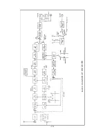
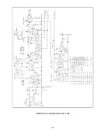
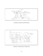
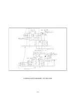
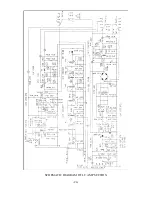
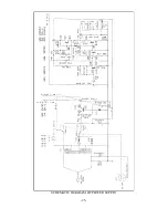
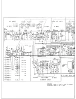
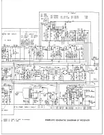
The complete circuit of the SX- 190 is shown in the schematic diagram at the rear of the manual. 
A block diagram is also provided to aid in understanding this receiver. While reading the text it 
is suggested that both diagrams be followed. The block diagram will reveal the overall scheme, 
whereas the schematic diagram will provide the detailed circuitry. 
 
 
3.2 

RF AMPLIFIERS AND HIGH FREQUENCY OSCILLATOR 

 
The RF signal received at the antenna is applied to the gate of Q1 (cascode RF Amplifier) thru 
the antenna input connector J1. The PRESELECTOR control is a 3-section air variable capacitor 
that tunes the gate and drain of the RF amplifier as well as the gate of the first mixer (Q4). The 
required tuning range of these circuits is obtained by switching an appropriate value of induc-
tance in parallel with the PRESELECTOR tuning capacitor and its associated coils (T1, T2, & 
T3). The complete range of 3.5 - 30 MHz is covered by 2 tuning ranges of the PRESELECTOR 
and by 11 ranges of the crystal controlled high frequency oscillator (Q5). The output of the high 
frequency oscillator (HFO) is coupled to the source of the 1st mixer as well as the base of an 
emitter follower (Q6), which is coupled to J2 on the rear panel of the receiver. The emitter fol-
lower allows the output of the HFO to be used without any loading effect being placed on the 
HFO. The RF GAIN control (VR1, 2) varies the AGC voltage fed to the base of the AGC Ampli-
fier Q2, and also attenuates the coupling between T1 and T2. As the setting is changed in a coun-
terclockwise direction, the bias decreases causing a reduction in gain of the RF amplifier stage. 
The same condition exists when the strength of the incoming signal increases. The output of the 
RF Amplifier is coupled by T2 and tuned by the PRESELECTOR tuning capacitor to the gate of 
Q4, the first mixer. 
 
The output of the HFO is always 2.920 MHz higher than the lower edge of the selected band. On 
frequencies below 17.920 MHz the oscillator collector circuit is tuned to the fundamental crystal 
frequency; at frequencies above 20.420 MHz the collector circuit is tuned to the third overtone of 
the crystal. 


-17- 

Summary of Contents for SX-190

Page 1: ......

Page 2: ...lt for 10 db S N ratio Sensitivity SSB CW Less than 0 5 microvolt for 10 db S N ratio Selectivity 4 KHz at 6 db down Visual dial accuracy 200 Hz Calibration accuracy Better than 500 Hz adjacent 25 KHz calibration points after indexing Stability Better than 500 Hz after warm up Image rejection More than 60 db Spurious rejection More than 50 db Rejection tuning More than 40 db Selection tuning 500 H...

Page 3: ...r calibrating the dial readout to an accuracy of better than 200Hz The SX 190 is equipped with a crystal controlled Beat Frequency Oscillator BFO for the recep tion of USB LSB and CW signals Incorporated in its circuitry are AGC ANL and S meter functions The AGC Automatic Gain Control has been tailored to produce minimum audio output changes even with large variations of input signal levels ANL Au...

Page 4: ...IVER CONNECTIONS If the SX 190 Receiver is to be used for receiving only and not as part of a system with intercon nections to an associated transmitter there are only a few required connections These connec tions are easily accessible at the rear of the receiver and their design permits permanent connec tions to be made in a neat manner Figure 1 2 page 5 illustrates the connections points at the ...

Page 5: ...he black to negative It is impor tant to observe the polarity when using the receiver on 12 VDC 1 2 5 STD BY CONNECTIONS The STD BY jack is jumpered in factory to operate the receiver 1 3 INTERCONNECTIONS FOR USE WITH TRANSMITTER Figure 1 1 page 5 illustrates the interconnections required for using SX 190 Receiver with a transmitter The following paragraphs describe the required interconnections t...

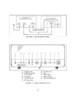
Page 6: ...INTERCONNECTIONS A Speaker jack G AC line cord B Line Tape output H Fuse C VFO output I HFO output D Ext std by J GND terminal E AC DC switch K 80 239 antenna jack F DC input jack FIGURE 1 2 REAR VIEW OF SX 190 5 ...

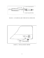
Page 7: ...FIGURE 1 3 ATTACHING CABLE TO PHONE PLUG CONNECTOR FIGURE 1 4 INSTALLATION OF GROUND 6 ...

Page 8: ...b Doublet Antenna A doublet antenna will give excellent results especially on amateur bands A 75 ohms balanced transmission line should be used as shown in Fig 1 5 2 Since the doublet antenna provides optimum performance only at a given frequency it should be cut to the length for the most often used band of frequencies The overall length of a doublet antenna can be determined by using the followi...

Page 9: ...tch J 100 kHz Calibrator switch C Band switch K AF gain control D Main tuning knob L RF gain control E Dial skirt M S meter F Main dial N Q multiplier switch G Preselector O Rejection tuning H Preselector dial P Phones jack FIGURE 2 1 FRONT VIEW OF SX 190 8 ...

Page 10: ...r Band C This an 11 position Band Change Switch to cover the international broadcasting bands from 3 5 to 18 0 MHz the 15 MHz standard frequency signal WWV and the 27 MHz CB band Tuning D E F This is the Main Tuning Knob One revolution controls a 50 KHz linear dial reading Each indi cation line on the knob indicates 1 KHz for frequencies between 3 5 and 30 0 MHz The dial skirt is held in place by ...

Page 11: ...m a local station may overload the receiver causing distortion and a resultant decrease in sound level K This is the volume control Turn to the right in a clockwise direction to increase vol ume and to the left to decrease volume S Meter Readings M The S Meter provides a means of measuring the relative strength of incoming signals Relative readings are only correct when the RF GAIN control is full...

Page 12: ...ity with which signal will be received will depend upon proper readjustment of the various controls Function Switch to SSB upper or lower for reception of SSB and CW and to AM for AM reception When pulse type interference hampers AM reception switch FUNCTION to AM ANL Band Set this switch to the desired band RF Gain Set this control for maximum sensitivity Full clock wise position AF Gain Adjust t...

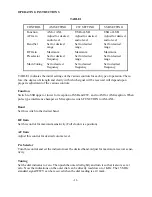
Page 13: ... then be adjusted on either side of the center for desired pitch Signal Sideband Operation For SSB reception the dial should be turned very slowly Excessive signal strength during SSB reception may make demodulation difficult In such cases decrease the RF GAIN by turning this control to the left Smooth demodulation will then be possible Control settings for sideband reception are virtually the sam...

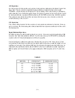
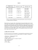
Page 14: ...e broadcast stations operate are found in the two upper bands of your receiver The majority of shortwave broadcast stations operate within certain internationally assigned groups of frequencies or bands For your convenience a list of the shortwave bands which offer best reception has been provided TABLE 3 Since shortwave reception varies with the time of day season of the year and with weather con...

Page 15: ...ing to other bands Q MULTIPLIER The Q multiplier operates in all modes CW AM and SSB to null unwanted signals with a deep 40 dB notch or peak the desired signal while sharpening receiver selectivity to help you pick the signal you want out of the noise The selector switch has off reject and select positions A tune control allows you to move the peak or null throughout the receiver bandpass When ce...

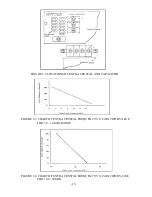
Page 16: ... 2 LOCATIONS OF EXTRA CRYSTAL AND CAPACITOR FIGURE 2 3 CHART OF EXTRA CRYSTAL FREQUENCY VS CAPACITOR VALUE FOR 3 5 10 MHz RANGE FIGURE 2 4 CHART OF EXTRA CRYSTAL FREQUENCY VS CAPACITOR VALUE FOR 10 0 30 MHz 15 ...

Page 17: ... 16 ...

Page 18: ...apacitor that tunes the gate and drain of the RF amplifier as well as the gate of the first mixer Q4 The required tuning range of these circuits is obtained by switching an appropriate value of induc tance in parallel with the PRESELECTOR tuning capacitor and its associated coils T1 T2 T3 The complete range of 3 5 30 MHz is covered by 2 tuning ranges of the PRESELECTOR and by 11 ranges of the crys...

Page 19: ...he bandpass IF and VFO are selected in the collector circuit of Q8 sec ond mixer The output of the VFO is provided at the rear panel at J4 Here the VFO is isolated by emitter follower Q10 3 5 455 KHz IF DETECTOR CIRCUITS AND NOISE LIMITER Immediately following the 2nd mixer Q8 are the mechanical Filters MF1 MF2 Output from the MF1 is amplified by Q13 and connects to MF2 and is tuned by the three t...

Page 20: ...an oscillator providing the necessary frequency to the bal anced demodulator for the beat between the 455 KHz IF signal In the LSB position of the Func tion switch X13 is in the circuit producing a frequency of 456 5 KHz In the USB position X12 produces a frequency of 453 5 KHz X Crystal 3 8 AGC AND S METER CIRCUITRY Signal voltage is coupled from the primary of T11 to AGC detector D6 and D7 The A...

Page 21: ...er amplifier transistor Q18 And every 100 KHz harmonic is supplied thru C80 Q19 and Q20 are multivibrators to oscillate at 25 kHz It is also connected to buffer ampli fier and to C80 3 11 POWER SUPPLY The power supply of the SX 190 has the advantage of operating from 120 VAC 60 Hertz or 12 VDC without any internal wiring changes 3 11 1 AC POWER SUPPLY Transformer T13 steps down the voltage from th...

Page 22: ...SCHEMATIC DIAGRAM OF RF AMP 21 ...

Page 23: ...SCHEMATIC DIAGRAM OF BUFFER AMP SCHEMATIC DIAGRAM OF CALIBRATOR 22 ...

Page 24: ...SCHEMATIC DIAGRAM OF VFO SECTION 23 ...

Page 25: ...SCHEMATIC DIAGRAM OF I F AMP SECTION 24 ...

Page 26: ...SCHEMATIC DIAGRAM OF POWER SUPPLY 25 ...

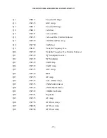
Page 27: ...Variable Frequency Osc Q10 2SC372 Variable Frequency Osc Emitter Follower Q11 2SC372 Q Multiplier Inverter Q12 2SC372 Q Multiplier Q13 2SC372 2nd IFAmp Q14 2SC372 2nd IF Amp Q15 2SC373 AGC Amp Q16 2SC372 BFO Q17 2SC373 AF Amp Q18 2SC373 CAL Buffer Amp Q19 2SC373 25khz Multivibrator Q20 2SC373 25kHz Multivibrator Q21 2SC372 100kHz Calibrator Q22 2SC971 Regulator Q23 2SC373 AF Amp Q24 2SC735 AF Driv...

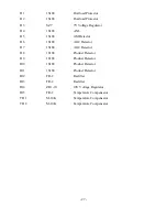
Page 28: ... 1S188 AGC Detector D 7 1S188 AGC Detector D 8 18188 Product Detector D 9 18188 Product Detector D10 1S188 Product Detector D11 1S188 Product Detector D12 FR 2 Rectifier D13 FR 2 Rectifier D14 ZB1 10 10V Voltage Regulator D15 FR 2 Temperature Compensator TH 1 M 10K Temperature Compensator TH 2 M 10K Temperature Compensator 27 ...

Page 29: ......

Page 30: ......

Page 31: ......

Reviews: