3.6 AUDIO
CIRCUITS
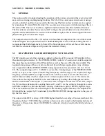
As stated earlier the audio voltage developed by a particular detector is coupled through the
Function switch (SW3-d) to the AF Gain control (VR3). The audio voltage is amplified in three
separate stages. The first audio amplifier Q23 feeds the second audio amplifier Q24 that drives
the final audio output stage, which is operating push-pull, and consists of transistors Q25 and
Q26.
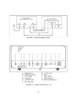
The audio system has been designed to provide three different audio outputs. J6 is an 8-ohm
phone output for a head-phone. Jack J7 is also an 8-ohm speaker jack. The third audio output J8
is a 600-ohm output jack, which can be used for tape out and/or line out operation.
3.7
BFO AND CW OSCILLATOR CIRCUITS
BFO circuitry consists of the transistor Q16 and it associated circuitry. In the reception of LSB
and USB signals the Function switch will place either X12 or X13 (USB or LSB) in the base cir-
cuit of Q16. Q16 now functions as an oscillator providing the necessary frequency to the bal-
anced demodulator for the beat between the 455 KHz IF signal. In the LSB position of the Func-
tion switch X13 is in the circuit producing a frequency of 456.5 KHz. In the USB position, X12
produces a frequency of 453.5 KHz.
(X: Crystal)
3.8
AGC AND "S" METER CIRCUITRY
Signal voltage is coupled from the primary of T11 to AGC detector D6 and D7. The AGC ampli-
fier Q15 amplifies the rectified signal voltage.
The collector voltage of Q15 is divided by R65 and VR2, and it is applied to the IF and RF am-
plifier stages. Emitter voltage of Q15 is used for "S" meter circuit.
The AGC time constant is controlled by C65 and thru C64. In the USB and LSB position the
parallel combination of C64 present a larger time constant resulting in a slower AGC discharge
rate.
The RF GAIN control VR2 provides a manual control of the gain in the RF, 1st, 2nd mixer and
IF stages. The RF Gain control is in series with the bases and controls static bias to these stages
As the control is rotated counter-clockwise the bias voltage decreases, reducing the bias and
therefore the gain of the stages.
-19-
Summary of Contents for SX-190
Page 1: ......
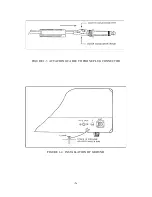
Page 7: ...FIGURE 1 3 ATTACHING CABLE TO PHONE PLUG CONNECTOR FIGURE 1 4 INSTALLATION OF GROUND 6 ...
Page 17: ... 16 ...
Page 22: ...SCHEMATIC DIAGRAM OF RF AMP 21 ...
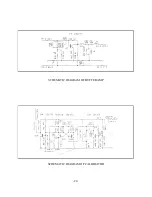
Page 23: ...SCHEMATIC DIAGRAM OF BUFFER AMP SCHEMATIC DIAGRAM OF CALIBRATOR 22 ...
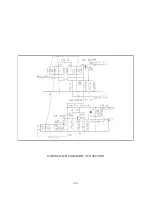
Page 24: ...SCHEMATIC DIAGRAM OF VFO SECTION 23 ...
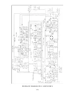
Page 25: ...SCHEMATIC DIAGRAM OF I F AMP SECTION 24 ...
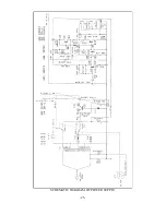
Page 26: ...SCHEMATIC DIAGRAM OF POWER SUPPLY 25 ...
Page 29: ......
Page 30: ......
Page 31: ......

