3.9 REJECTION
FILTER
The Rejection Filter consists of transistors Q11, Q12 and their associated components. The fre-
quency of the notch is controlled by VC7, REJECTION TUNING. This control allows the notch
to be moved across the passband of the 455 KHz IF. Resistor, VR15, is used to adjust the depth
of the notch.
This notch circuit is an inverted "Q" multiplier. The circuitry around Q12 multiplies the "Q" of
coil T7. By multiplying its "Q", the circuit provides a narrower notch. This circuit shapes the
notch and VR15 sets the depth. The output of this circuit is actually a peak rather than a notch
until it is inverted by Q11, then it appears as a notch when tuned through the IF passband.
3.10 CALIBRATION
CIRCUIT
Calibration circuitry consists of transistors Ql8 thru Q21. 100 KHz signal is produced by Q21
and connected to buffer amplifier transistor Q18. And every 100 KHz harmonic is supplied thru
C80. Q19 and Q20 are multivibrators to oscillate at 25 kHz. It is also connected to buffer ampli-
fier and to C80.
3.11 POWER
SUPPLY
The power supply of the SX-190 has the advantage of operating from 120 VAC 60 Hertz or 12
VDC without any internal wiring changes.
3.11.1 AC POWER SUPPLY
Transformer T13 steps down the voltage from the source to a nominal voltage of approximately
10 Volts. This voltage is then rectified by the diode consisting of diodes D12 and Dl3. This recti-
fied voltage is then fed to the collector Q22. In the base circuit of Q22, a 10V Zener regulator is
used to regulate the base potential. Transistor Q22 is used as an emitter follower regulator. From
here the 9.5V supply line is taken, and also the 7V supply line originates thru a dropping resistor
R82. The 7V supply line is regulated by a 7V Zener Diode D3.
3.11.2 DC POWER SUPPLY
There is no DC power supply as such. The receiver merely regulates and fuses the 12 VDC
source.
- 20 -
Summary of Contents for SX-190
Page 1: ......
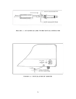
Page 7: ...FIGURE 1 3 ATTACHING CABLE TO PHONE PLUG CONNECTOR FIGURE 1 4 INSTALLATION OF GROUND 6 ...
Page 17: ... 16 ...
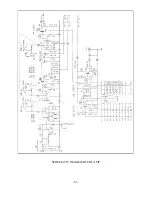
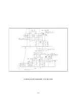
Page 22: ...SCHEMATIC DIAGRAM OF RF AMP 21 ...
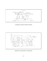
Page 23: ...SCHEMATIC DIAGRAM OF BUFFER AMP SCHEMATIC DIAGRAM OF CALIBRATOR 22 ...
Page 24: ...SCHEMATIC DIAGRAM OF VFO SECTION 23 ...
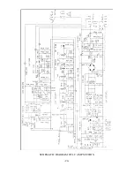
Page 25: ...SCHEMATIC DIAGRAM OF I F AMP SECTION 24 ...
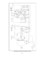
Page 26: ...SCHEMATIC DIAGRAM OF POWER SUPPLY 25 ...
Page 29: ......
Page 30: ......
Page 31: ......

