background image

ADM-SDEV-BASE/XCKU060 User Manual
V1.0 - 27th November 2018

1 Introduction

The ADM-SDEV-BASE/XCKU060 shall be the base board at the core of the ADA-SDEV-KIT1 space FPGA

development kit, enabling customers interested in space grade FPGAs to prototype their applications on a

compatible XCKU060-1I device.

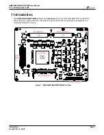
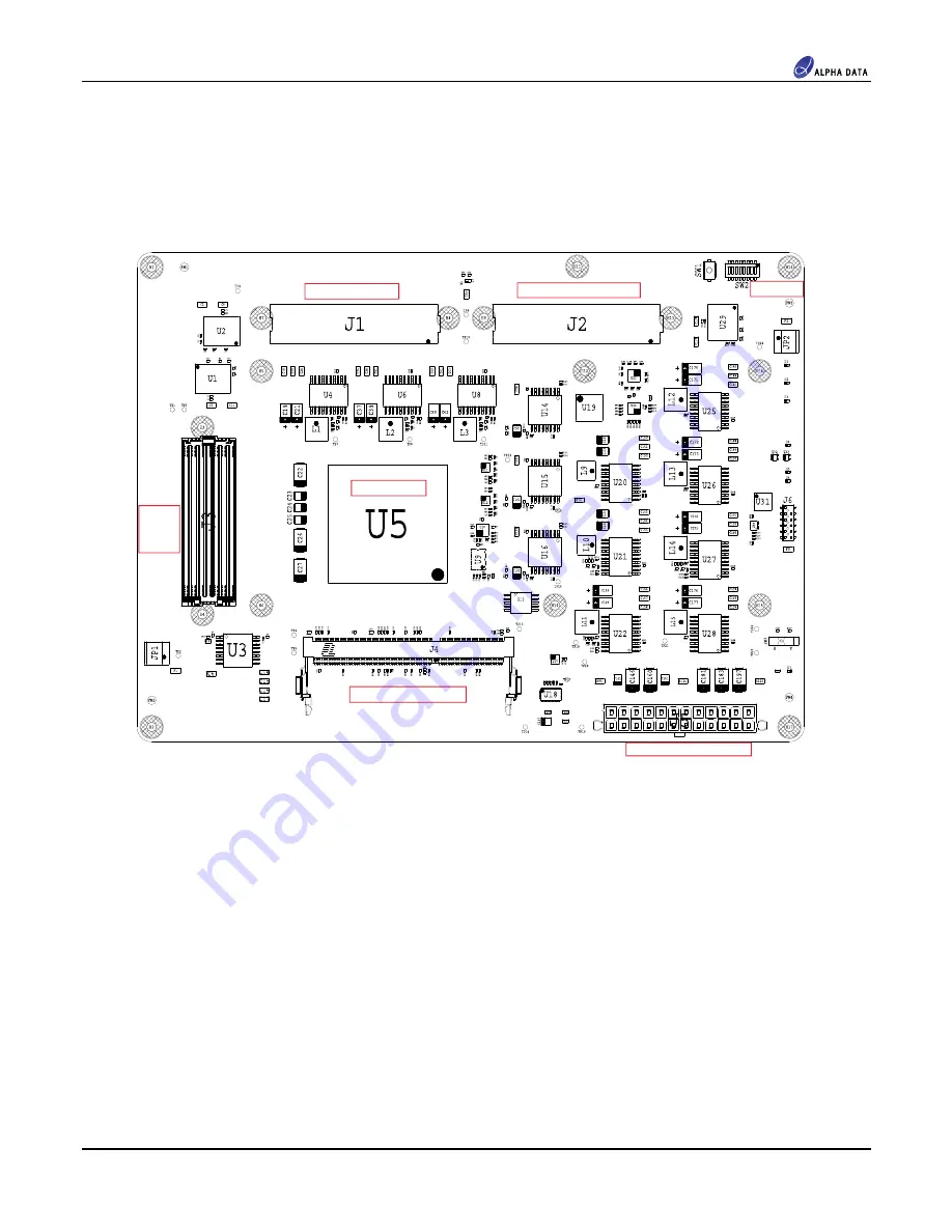
LPC FMC Socket

CONFIG FMC Socket

KU060 FPGA

HPC
FMC+
Socket

DDR3 SODIMM Socket

ATX Power Connector

Switches

Figure 1 : ADM-SDEV-BASE/XCKU060 Top View

Page 1

Introduction
ad-ug-1360_v1_0.pdf

Summary of Contents for ADM-SDEV-BASE/XCKU060

Page 1: ...ADM SDEV BASE XCKU060 User Manual Document Revision 1 0 27th November 2018...

Page 2: ...y shape or form without prior written consent from Alpha Data Parallel Systems Ltd Head Office Address 4 West Silvermills Lane Edinburgh EH3 5BD UK Telephone 44 131 558 2600 Fax 44 131 558 2700 email...

Page 3: ...o Carrier Global Clocks CLK_M2C 9 3 3 4 Module to Carrier MGTREF Clocks GBTCLK_M2C 10 3 4 Configuration 11 3 4 1 Configuration From ADM SDEV CFG1 Flash Memory 11 3 4 1 1 Building and Programming Confi...

Page 4: ...arget MGT Links 15 Table 14 LPC FMC Groups J1 18 Table 15 Config FMC Groups J2 18 Table 16 FMC Groups J3 18 List of Figures Figure 1 ADM SDEV BASE XCKU060 Top View 1 Figure 2 ADM SDEV BASE XCKU060 Blo...

Page 5: ...DA SDEV KIT1 space FPGA development kit enabling customers interested in space grade FPGAs to prototype their applications on a compatible XCKU060 1I device LPC FMC Socket CONFIG FMC Socket KU060 FPGA...

Page 6: ...ger configuration and debug requires ADM SDEV CFG1 board Programmable clock generation controlled by I2C connected to the FMC config daughter base board and the FPGA Heatsink and Fan on top of KU060 F...

Page 7: ...draws all of its power from the 5V rail Some ATX power supplies may not operate without a minimum load on the 3 3V rail which will require a configuration change on the ADA SDEV BASE board Please con...

Page 8: ...C 1 LPC Q227 Q228 Q224 Q225 Q226 Q128 Q127 Q126 JTAG 45 44 66 67 68 47 24 48 25 46 64 65 x2 x4 x4 x3 x4 x4 x4 x4 x1 Power Supplies Programmable Clock Generator DDR3 SODIMM FMC 2 Config x4 Serial IO IP...

Page 9: ...normal operation Switch Ref Function ON State Off State SW1 push button Reset System Reset Normal Operation SW2 1 Reserved Normal Operation SW2 2 Reserved Normal Operation SW2 3 Config Disable Configu...

Page 10: ...State Off State D1 Green Status 0 See Status LED Definitions D2 Red Status 1 See Status LED Definitions D3 Red Internal Power Fault Internal Power supply fault Normal operation D4 Green FPGA Done FPGA...

Page 11: ...DR_TDO Level Shift 3V3 FMC2_VIO FMC2_TDI FMC2_TDO Config FMC J2 FMC J3 FMC3_PRESENT Level Shift FMC2_VIO 3V3 En FMC3_TDI FMC3_TDO FPGA_TDO Figure 4 JTAG Boundary Scan Chain At each stage the clock sig...

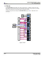
Page 12: ...MGT Banks MGT228 REFCLK0 REFCLK1 MGT227 REFCLK0 REFCLK1 MGT226 REFCLK0 REFCLK1 MGT225 REFCLK0 REFCLK1 MGT224 REFCLK0 REFCLK1 MGT128 REFCLK0 REFCLK1 MGT127 REFCLK0 REFCLK1 User Programmable Source 0 MG...

Page 13: ...ents Signal Frequency Target FPGA Input IO Standard P pin N pin PROGCLK0 0 5 400 MHz IO BANK 45 LVDS AL27 AL28 PROGCLK0 1 5 400 MHz MGTREFCLK1_224 LVDS AP10 AP9 PROGCLK0 2 5 400 MHz MGTREFCLK1_127 LVD...

Page 14: ...nections 3 3 4 Module to Carrier MGTREF Clocks GBTCLK_M2C Each connected FMC board can generate a number of differential MGT Reference clocks as per the FMC standard They each connect to an MGTREFCLK...

Page 15: ...MiB Start Address Bytes 0x000_0000 0x200_0000 Figure 6 Flash Address Map At power on the FPGA attempts to configure itself automatically in serial master mode based on the contents of the header in t...

Page 16: ...from the write_cfgmem tcl command 3 4 2 Configuration via JTAG A Xilinx Platform Programming Cable may be attached to the programming header on the Config FMC board This permits the FPGA to be reconfi...

Page 17: ...Input Supply 5 0V Board Input Supply 3 3V Board Input Supply FMC2_VIO Config FMC I O voltage 2 5V Level Translation 1 8V FPGA IO Voltage VCCO 0 95V Target FPGA Core Supply VccINT 1 8V Target Transceiv...

Page 18: ...switching off and the two status LEDs showing a temperature fault indication The purpose of this mechanism is to protect the card from damage due to over temperature 3 5 2 Microcontroller Status LEDs...

Page 19: ...24 64 FMC2_VADJ Config FMC GPIO 25 46 47 FMC3_VADJ FMC GPIO 48 FMC3_VIO_B FMC GPIO 66 67 68 1 5V DDR SODIMM Table 12 Target FPGA IO Banks 3 6 2 Target MGT Links There are a total of 32 Multi Gigabit T...

Page 20: ...scale MGT MGT126 MGT127 MGT227 MGT226 MGT225 MGT224 Config FMC J2 FMC J3 MGT128 MGT228 FMC2_DP 3 0 FMC1_DP 3 0 LPC FMC J1 FMC3_DP 3 0 FMC3_DP 7 4 FMC3_DP 11 8 FMC3_DP 15 12 FMC3_DP 19 16 FMC3_DP 23 20...

Page 21: ...66 67 68 The memory banks are arranged for compatibility with the Xilinx Memory Interface Generator MIG DRAM Banks Shows the FPGA banks used Full details of the interface signaling standards and an e...

Page 22: ...16 2 15 diff Pairs 30 single ended FMC2_LA_CC 1 0 2x Regional Clocks GPIO pairs 4 single ended FMC2_LA_1 64 FMC2_LA 33 19 15 diff Pairs 30 single ended FMC2_LA_CC 18 17 2x Regional Clocks GPIO pairs...

Page 23: ...6 7 10 diff Pairs 20 single ended FMC3_HB 21 18 4 diff Pairs 8 single ended FMC3_HB_CC 0 Regional Clock GPIO pair 2 single ended FMC3_HB_CC 6 Regional Clock GPIO pair 2 single ended FMC3_HB_CC 17 Regi...

Page 24: ...er review 27 Nov 2018 1 0 First Release Address 4 West Silvermills Lane Edinburgh EH3 5BD UK Telephone 44 131 558 2600 Fax 44 131 558 2700 email sales alpha data com website http www alpha data com Ad...

Reviews: