ADM-VPX3-9V2 User Manual
3.2 VPX P0
3.2.1 Global Address
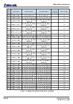
All global address pins are available as inputs to the FPGA.
See net names FPGA_GA* in section
for location details.
3.2.2 System Reset
SYSRESET# provides an input to the FPGA at the dedicated PERSTN0 pin for use with PCIe or general resets.
SYSRESET# can also be driven through an open drain buffer by the FPGA at net SYSRESET_OUT_L which can
3.2.3 REFCLK
VPX REFCLK is an optional VPX input/output that should be either a 25MHz or a 100MHz reference clock. By
default this clock is forwarded to MGTREFCLK0 of quad 224.
When REFCLK is 25MHz, it can be used as the clock source for all internally generated clocks. This is done by
setting SW1-3 on the debug board to ON, or through a build option.
The net REFCLK_OUT_EN_1V8 when driven high, will change the external REFCLK transceiver into an output
driver, and forward the net SE_REFCLK_OUT_1V8 onto the VPX backplane.
for location details.
3.2.4 AUXCLK
VPX AUXCLK is an optional VPX input/output that can provide an external reference timing pulse or clock. By
default this clock is forwarded as net name AUXCLK_SE_1V8 GPIO in FPGA bank 64.
The net AUXCLK_DIR_1V8 when driven high, will change the external AUXCLK transceiver into an output driver,
and forward the net AUXCLK_SE_1V8 onto the VPX backplane.
for location details.
3.2.5 Management Bus (SM0-SM3)
The default build option sends SM0-SM3 to the FPGA for user implementation at net locations
IPMB0_FPGA_SCL, IPMB0_FPGA_SDA, IPMB1_FPGA_SCL, IPMB1_FPGA_SDA found in
SM0-SM3 are buffered through a LTC4309IDE I2C bus level translator to ensure high impedance isolation during
partial power-down.
SM0-SM3 can be controlled by the onboard system management microcontroller, but this requires a small
resistor population change controlled by a build modification.
for location details.
3.2.6 NVMRO
NVMRO is available as an input at net NVMRO_FPGA.
NVMRO can also be connected to the configuration flash memory through a build option upon request. Note that
this will increase the power-on configuration time for the FPGA by a factor of 2.
for location details.
Page 10
Functional Description
ad-ug-1377_v1_2.pdf


