ADM-VPX3-9V2 User Manual
3.3 VPX P1 and P2
3.3.1 Differential Pairs
All differential wafers in P1 and P2 are connected directly to high speed transceivers on the FPGA. These
connectors use RT3 VPX connectors which are capable of up to 28Gbps line rates. The FPGA is very flexible,
and these 32 lanes can be configured as any combination of 32 ultra-thin-pipes, 16 thin-pipes, 8 fat-pipes, or 4
ultra-fat-pipes as defined in the VPX specifications. These wafers can support protocols like 100G ethernets,
SRIO, Infiniband, or any other protocol supported directly by the Xilinx GTY Transceivers. Please see Xilinx User
Guide UG578 for more details on the capabilities of the transceivers.
All VPX differential lines (both RX and TX) have 220nF AC coupling capacitors in line for the most flexibility.
Alpha Data can change the value of these capacitors, or change them to 0 ohm resistors upon request.
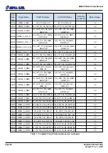
See
for quad and wafer mapping. Net nomenclature is shown below:
Wafer connections
•
P1 Wafers 1-8: PCIE_*
•
P1 Wafers 9-14: P1_*
•
P1 Wafer 15: ETH2_*
•
P1 Wafer 16: ETH1_*
•
P2 Wafers 1-16: P2_*
for location details.
3.3.2 P1 GDISC1#
GDiscrete1 is an optional, bidirectional, open drain, IO pin defined in the VPX specification at P1 pin G1. It is
controlled at the FPGA by net GDiscrete1_OUT and GDiscrete1_IN, both of which have external pull-ups. An
external open-drain buffer passes and receives logical low signals from the shared backplane bus to the FPGA.
Locations for these net names can be located in section
3.3.3 VBAT
VBAT is connected through a resistor divider to the FPGA VBAT pin, and can provide voltage to hold encryption
keys for secure boot load.
3.3.4 SYSCON#
The system controller input is buffered and sent to the FPGA as net SYSCON_1V8_L. The ADM-VPX3-9V2 has
some system controller functionality build in (REFCLK, management bus flexibility, SYSRESET control, etc.), and
can perform this function in some chassis.
3.3.5 MP01
The OpenVPX MP01 serial port at P1.G9 and P1.G11 is configurable as either 3.3V UART (default) or optionally
RS232 signaling levels (with build option). See net names UART_0_* and RS232_0 in
pin locations.
3.3.6 AX_RESETL#
This input is unused by default, and requires a build option to use this signal.
3.3.7 MSKRST#
The VPX maskable reset is combined with the system reset and sent to the dedicated PERSTN0 pin of the
FPGA. This is an ideal way to perform PCIe reset, or general logic resets.
Page 11
Functional Description
ad-ug-1377_v1_2.pdf


