ADM-VPX3-9V2 User Manual
3.3.8 P2 GPIO
All 8 user defined pins on row G of P2 are controllable through an SN74AVC4T774RSVR bidirectional buffer with
an external pull-up. The buffers are enabled with active low net P2_GPIO_EN_L (there is an external pull-up).
Each line has a directional control pin P2_GPIO_G*_DIR. DIR set high drives a GPIO out onto the backplane,
and logical low receives in from the backplane (there is an external pull-down). Nets P2_GPIO_*_1V8 are the
input/output pins to send and receive data.
MP02 at P1 pins G1 and G3 can be used as a serial 3.3V UART interface as per OpenVPX when configured with
the appropriate input and output directions.
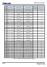
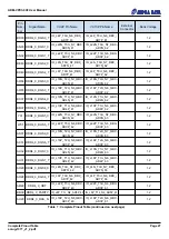
Locations for these net names can be located in section
3.3.9 MP02
The OpenVPX MP02 serial port at P2.G1 and P2.G3 is configurable as either 3.3V UART (default) or optionally
RS232 signaling levels (with build option). See net names GPIO_G1_1V8, GPIO_G3_1V8, and RS232_1* in
Page 12
Functional Description
ad-ug-1377_v1_2.pdf


