ADM-VPX3-9V2 User Manual
3.4 Clocking
The ADM-VPX3-9V2 provides flexible reference clock solutions for the many multi-gigabit transceiver quads and
FPGA fabric. Any programmable clock, from the SI5338 Clock Synthesizer, is re-configurable from the debug
board
by using Alpha Data’s avr2util utility. This allows the user to configure almost any arbitrary
clock frequency during application run time. The maximum clock frequency is 312.5MHz. Customers who utilize
Alpha Data SDK and API also have the option of embedding IP into their FPGA design that permits
programmable clock re-configuration via PCIe or from within the FPGA.
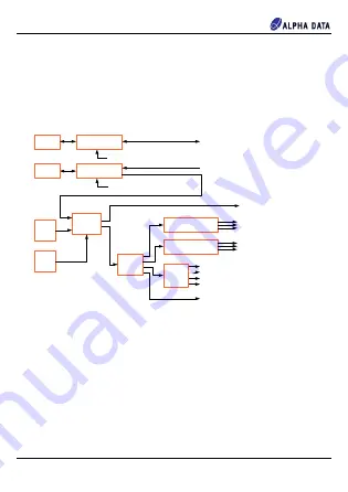
All clock names in the section below can be found in
FABRIC_CLK 300MHz (IO Bank 66)
25MHz
30ppm
Source
Si5338
Clock
Synth
AUXCLK_SE_1V8 (BANK 64)
0
1
2
3
AUXCLK_DIR_1V8 (BANK 64)
VPX
REFCLK
M-LVDS Buffer
SN65MLVD201DR
Buffer
CDCLVD110ARHBT
PROGCLK_0
All Connected MGTs
MGTREFCLK0 (except 224)
REFCLK300M_0 (BANK 61)
VPX
AUXCLK
M-LVDS Buffer
SN65MLVD201DR
SE_REFCLK_OUT_1V8 (BANK 64)
REFCLK_OUT_EN_1V8 (BANK 64)
NB6L72MN
Crosspoint
Switch
DEBUG
BRD
SW1-1
CLK_SEL
0
...
9
MGTREFCLK0_224
Must be
25MHz
Buffer
CDCLVD110ARHBT
PROGCLK_1
All Connected MGTs
MGTREFCLK1
0
...
9
Buffer
NB6L14S
REFCLK300M_1 (BANK 65)
REFCLK300M_2 (BANK 71)
REFCLK300M_3 (BANK 74)
For REFCLK as PCIe reference
DDR4 reference clocks
MGT reference clocks
MGT reference clocks
Figure 9 : Clock Topology
Page 13
Functional Description
ad-ug-1377_v1_2.pdf


