ADM-XRC-5T2-ADV User Manual
ADM-XRC-5T2-ADV User Manual
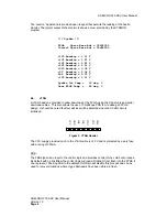
The ‘sysmon’ application is provided upon request that permits the reading of the health
monitor. The typical output of the monitor is shown below, provided by the SYSMON
program.
*** SysMon ***
FPGA Space Base Adr = 00900000
Control Space Base Adr = 00d00000
+1V0 Reading = 1.01 V
+1V2 Reading = 1.21 V
+1V8 Reading = 1.81 V
+2V5 Reading = 2.51 V
+3V3 Reading = 3.32 V
+5V Reading = 5.04 V
Pn4 Reading = 3.31 V
+1V5 Reading = 1.51 V
SysMon Int Temp = 33 deg. C
User FPGA Temp = 26 deg. C
4.4.
JTAG
A JTAG header is provided to allow download of the FPGA using the Xilinx tools and serial
download cables. This also allows the use of ChipScope PRO ILA to debug an FPGA
design. It should be noted that four devices will be detected when the SCAN chain is
initialised.
TM
S
TDI
TDO
FBS
TCK
GN
D
VCC
Figure 3 JTAG Header
The VCC supply provided on J5 to the JTAG cable is +3.3V and is protected by a poly fuse
with a rating of 350mA.
FBS
The FBS signal is an input to the control logic and provides control of the cold boot process.
By default with no link fitted, the control logic will load a bitstream from flash into the FPGA if
one is present. Shorting FBS to the adjacent GND pin will disable this process and can be
used to recover situations where rogue bitstreams have been stored in flash.
Version 1.0
Page 6


