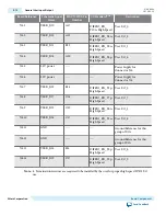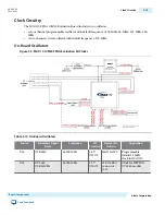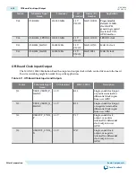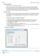
To configure the MAX 10 FPGA:
1. Start the Quartus II Programmer.
2. Click Add File and select the path to the desired .sof.
3. Turn on the Program/Configure option for the added file.
4. Click Start to download the selected file to the FPGA. Configuration is complete when the progress
bar reaches 100%.
The Quartus II Convert Programming File (CPF) GUI can be used to generate a .sof file that can use for
internal configuration. You can directly program the MAX 10 device’s flash which includes Configuration
Flash Memory (CFM) and User Flash Memory (UFM) by using a download cable with the Quartus II
software programmer.
Selecting the Internal Configuration Scheme
For all MAX 10 devices, except 10M02 device, there are total of 5 different modes you can select internal
configuration. Please refer to
Figure 2-2: Configuration Flash Memory Sectors Utilization for all MAX 10
Devices Except for 10M02 Device
of
MAX 10 FPGA Configuration User Guide
. You can access the PDF
of the MAX 10 FPGA Configuration User guide
here
.
The internal configuration scheme needs to be selected before design compilation. To select the
configuration mode:
1. Open the Quartus II software and load a project using MAX 10 device family.
2. On the Assignments menu, click Settings. The Settings dialog box appears.
3. In the Category list, select Device. The Device page appears.
4. Click Device and Pin Options.
5. In the Device and Pin Options dialog box, click the Configuration tab.
6. In the Configuration Scheme list, select Internal Configuration.
7. In the Configuration Mode list, select 1 out of 5 configuration modes. For the dual-boot feature:
a. Must have a Dual Boot IP in the design, for example, in a Qsys component.
b. Choose Dual Compressed Images (512 Kbits UFM) for the Configuration Mode.
c. Generate two .sof files above and convert them into one .pof file for CFM programming.
8. Turn on Generate compressed bit-streams if needed, and click OK.
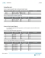
Status Elements
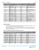
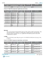
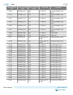
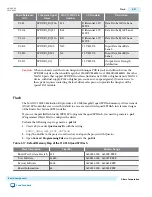
This topic lists the non-user status elements for the MAX 10 10M50 FPGA Evaluation Board.
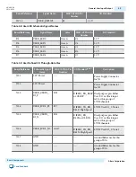
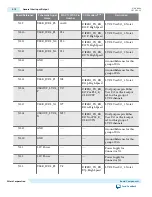
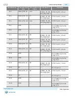
Table 3-3: Status LED Signal Names
Board Reference
Signal Name
Colour
Device/Pin Number
I/O Standard
D8
MAXII_CONF_
DONE
Green
MAX II / Y10
3.3 V
D9
5V_LED_R
Yellow
---
---
D10
2.5V_LED_R
Yellow
---
---
D11
1.2V_LED
Yellow
MAX II / Y9
3.3 V
UG-20006
2016.02.29
Selecting the Internal Configuration Scheme
3-7
Board Components
Altera Corporation
Send Feedback


