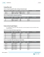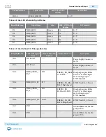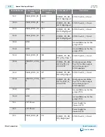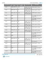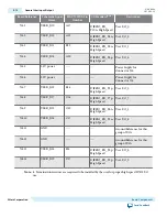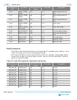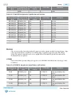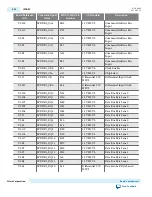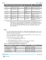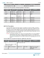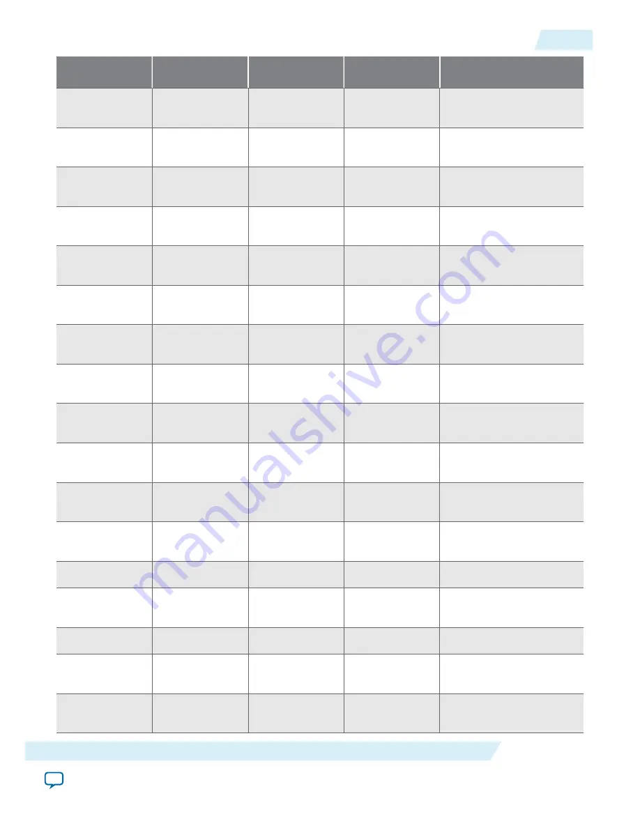
Board Reference
Schematic Signal
Name
MAX 10 FPGA Pin
Number
I/O Standard
Note 1
Description
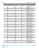
J13.4
USER_LVDS_P8
AA7
DIFFIO_TX_RX_
B16p, High Speed
LVDS User I/O_8. Note 1
J13.5
USER_LVDS_N5 V7
DIFFIO_TX_RX_
B7n, High Speed
LVDS User I/O_5. Note 1
J13.6
USER_LVDS_N8 AA6
DIFFIO_TX_RX_
B16n, High Speed
LVDS User I/O_8. Note 1
J13.7
GND
----
----
Ground Reference for this
group of I/Os
J13.8
GND
----
----
Ground Reference for this
group of I/Os
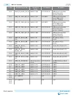
J13.9
USER_LVDS_P6
W6
DIFFIO_TX_RX_
B1p, High Speed
LVDS User I/O_6. Note 1
J13.10
USER_LVDS_P4
W10
DIFFIO_TX_RX_
B11p, High Speed
LVDS User I/O_4. Note 1
J13.11
USER_LVDS_N6 W5
DIFFIO_TX_RX_
B1n, High Speed
LVDS User I/O_6. Note 1
J13.12
USER_LVDS_N4 W9
DIFFIO_TX_RX_
B11n, High Speed
LVDS User I/O_4. Note 1
J13.13
GND
----
----
Ground Reference for this
group of I/Os
J13.14
GND
----
----
Ground Reference for this
group of I/Os
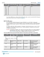
J13.15
USER_LVDS_P7
W3
DIFFIO_TX_RX_
B5p, High Speed
LVDS User I/O_7. Note 1
J13.16
NC
----
----
Not Connected
J13.17
USER_LVDS_N7 W4
DIFFIO_TX_RX_
B5n, High Speed
LVDS User I/O_7. Note 1
J13.18
NC
----
----
Not Connected
J13.19
GND
----
----
Ground Reference for this
group of I/Os
J13.20
GND
----
----
Ground Reference for this
group of I/Os
UG-20006
2016.02.29
General User Input/Output
3-11
Board Components
Altera Corporation
Send Feedback


