background image

Table 3-12: The Clock Control Tab

Control

Description

F_vco

Displays the generating signal value of the voltage-controlled

oscillator

Registers

Display the current frequencies for each oscillator

Frequency (MHz)

Allows you to specify the frequency of the clock

Disable

Disable each oscillators as required

Read

Reads the current frequency setting for the oscillator associated

with the active tab

Default

Sets the frequency for the oscillator associated with the active

tab back to its default value. This can be also be accompanied

by power cycling the board.

Set New Freq

Sets the programmable oscillator frequency for the selected

clock to the value in the CLK0 and CLK3 controls. Frequency

changes might take several milliseconds to take effect. You

might see glitches on the clock during this time. Altera

recommends resetting the FPGA logic after changing frequen‐

cies.
Note: Changing CLK0 of Si5338 will affect the Clock/

Power GUI. Once clock from Port CLK0 is used to

drive the MAX II device which is working as a 2-

wire serial bus interface connected to Si570, Si5338

and power monitor.

Components and Interfaces

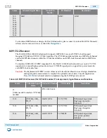
This section describes the evaluation board's ports and optional interface cards relative to the MAX 10

FPGA device.

HDMI Video Output

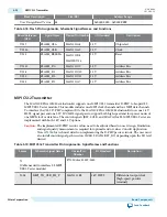
The MAX 10 10M50 evaluation kit supports one HDMI transmitter and one HDMI receptacle. The

transmitter incorporates HDMI v1.4 features, and is capable of supporting an input data rate up to 165

MHz (1080p @ 60Hz, UXGA @ 60Hz). The connection between HDMI transmitter and MAX 10 is

established in Bank 7, and the communication can be done via I2C interface.

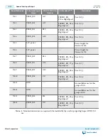
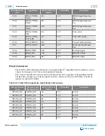
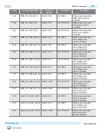
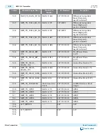
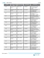
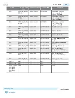
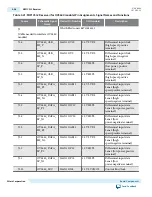
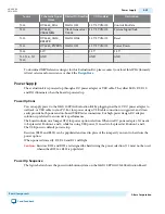
Table 3-13: HDMI Pin Assignments, Signal Names and Functions

Board Reference

(U3)

Signal Name

MAX 10 FPGA Pin

Number

I/O Standard

Description

U3.62

HDMI_VIDEO_

DIN0

J12

3.3 V

HDMI digital video data

bus

3-16

Components and Interfaces

UG-20006

2016.02.29

Altera Corporation

Board Components

Send Feedback

Summary of Contents for MAX 10 FPGA 10M50

Page 1: ...MAX 10 FPGA 10M50 Evaluation Kit User Guide Subscribe Send Feedback UG 20006 2016 02 29 101 Innovation Drive San Jose CA 95134 www altera com ...

Page 2: ...g the Quartus II Programmer 3 6 Selecting the Internal Configuration Scheme 3 7 Status Elements 3 7 Setup Elements 3 8 General User Input Output 3 8 Clock Circuitry 3 13 On Board Oscillators 3 13 Off Board Clock Input Output 3 14 Clock Control GUI 3 15 Components and Interfaces 3 16 HDMI Video Output 3 16 Pmod Connectors 3 18 Memory 3 19 Flash 3 21 MIPI CSI 2 Transmitter 3 22 MIPI CSI 2 Receiver 3...

Page 3: ...Synchronous Buck DC DC Converter with Integrated Inductor FPGA configuration Embedded USB Blaster II JTAG Optional JTAG direct via 10 pin header On Board clocking circuitry 25 MHz single ended external oscillator clock source Silicon Labs Si510 crystal oscillator Silicon Labs Si5338 clock generator with programmable frequency GUI Memory devices 64M x 16 1Gbits LPDDR2 with soft memory controller 51...

Page 4: ... SW2 1 SW2 2 Power Yellow Power ON LEDs D9 D10 D11 USB Y cable USB Type A to mini Type B for both on board USB Blaster II and 5V 1A power capability Support DC power adapter option but 5V power supply and cord are not included in the kit Software Free Quartus Prime Lite Edition design software download software and license from http www altera com download Complete documentation User Guide bill of...

Page 5: ...ms are sold separately Table 1 1 Additional Components Not Included with the Kit Board Reference Description Manufacturer Manufacturing Part Number Manufacturer Website J1 J2 Cable Flat Flex Top Top 36 POS 0 5 MM pitch Parlex Molex Leopard Imaging 050R36 76B 0210200385 LI FLEX03 www parlex com www molex com www leopardi maging com UG 20006 2016 02 29 Supported Items Not Included with the Kit 1 3 M...

Page 6: ...ster II Download Cable Altera PL USB2 BLASTER https www altera com products boards_and_ kits download cables html J10 Standard 5V 2 0A Switching Power Adapter LI Tone Electronics LTE12E S1 316 www lte com tw J10 Standard 5V 3 0A Switching Power Adapter Huntkey HKA08105030 8B http dealer huntkey com en J1 LI MIPI USB Tester Daughter Card Leopard Imaging LI USB30 MIPI TESTER http shop leopardi magin...

Page 7: ... website On the Altera Programming Cable Driver Information page of the Altera website locate the table entry for your configuration and click the link to access the instructions Handling the Kit When handling the board it is important to observe the following static discharge precaution Caution Without proper anti static handling the board can be damaged Therefore use anti static handling precaut...

Page 8: ...Board Reference Signal Name Function Default Position SW1 1 USER_DIPSW0 User Defined HIGH OFF 1 SW1 2 USER_DIPSW1 User Defined HIGH OFF 1 SW1 3 USER_DIPSW2 User Defined HIGH OFF 1 SW1 4 USER_DIPSW3 User Defined HIGH OFF 1 Table 2 2 Default SW2 DIP Switch Settings Board Reference Signal Name Function Default Position SW2 1 USER_DIPSW4 User Defined HIGH OFF 1 2 2 Factory Default Switch and Jumper Se...

Page 9: ...vice is provided within the On board USB Blaster II it provides access to diagnostic hardware and board identifica tion information The device shows up as an extra device on the JTAG chain with ID 020D10DD This switch removes the virtual JTAG device from the JTAG chain HIGH OFF 1 Table 2 3 Default J11 Jumper Settings Jumper Function Setting J11 1 2 Jumper for board DC adapter power option when R29...

Page 10: ...Corporation and registered in the U S Patent and Trademark Office and in other countries All other words and logos identified as trademarks or service marks are the property of their respective holders as described at www altera com common legal html Altera warrants performance of its semiconductor products to current specifications in accordance with Altera s standard warranty but reserves the ri...

Page 11: ...Figure 3 1 Overview of the MAX 10 10M50 FPGA Evaluation Kit Features Board Image Front View 3 2 Board Overview UG 20006 2016 02 29 Altera Corporation Board Components Send Feedback ...

Page 12: ...ption Featured Device U1 FPGA MAX 10 FPGA 10M50DAF484C6GES 50K LEs F484 package 6ES speed grade U13 CPLD MAX II EPM1270 256 MBGA 2 5V 3 3V VCCINT for On Board USB Blaster II U17 Power Regulator Enpirion EN5329QI 2A PowerSoC Low Profile Synchronous Buck DC DC Converter with Integrated Inductor UG 20006 2016 02 29 Board Overview 3 3 Board Components Altera Corporation Send Feedback ...

Page 13: ...nfigure from on die Configuration Flash Memory CFM S7 FPGA register push button Toggling this button resets all registers in the FPGA J11 Jumper for board power option Default connection is Pins 2 and 3 position which uses USB power supply If needed change jumper position to Pins 1 and 2 for DC adapter power supply solution Status Elements D8 Configuration done LED green Illuminates when the FPGA ...

Page 14: ...up to 1080p through an ADI Analog Devices Inc HDMI transmitter ADV7513 I O and Expansion Ports J8 J9 Two Diligent Pmod connectors 12 pin interface with 8 I O signal pins used to connect low frequency low I O peripheral modules J12 J13 Two 2x10 GPIO connectors user install You can use this area to connect or solder additional components for connection of 9 true LVDS pairs with clock input and outpu...

Page 15: ...e to the FPGA Any subsequent power cycling of the FPGA or reconfiguration will power up the FPGA to a blank state Programming of the on die FPGA Configuration Flash Memory CFM via a pof file Any power cycling of the FPGA or reconfiguration will power up the FPGA in self configuration mode using the files stored in the CFM You can use two different USB Blaster hardware components to program the sof...

Page 16: ...esign compilation To select the configuration mode 1 Open the Quartus II software and load a project using MAX 10 device family 2 On the Assignments menu click Settings The Settings dialog box appears 3 In the Category list select Device The Device page appears 4 Click Device and Pin Options 5 In the Device and Pin Options dialog box click the Configuration tab 6 In the Configuration Scheme list s...

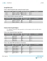
Page 17: ...mes FPGA pin numbers and I O standards for the MAX 10 FPGA 10M50 Evaluation Board Table 3 6 User Defined Push Button Signal Names Board Reference Signal Name MAX 10 FPGA Pin Number I O Standard S1 USER_PB0 R20 1 2 V S2 USER_PB1 Y20 1 2 V S3 USER_PB2 Y21 1 2 V S4 USER_PB3 U20 1 2 V Table 3 7 User Defined DIP Switch Schematic Signal Names Board Reference Signal Name MAX 10 FPGA Pin Number I O Standa...

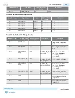
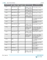
Page 18: ...ower Supply Connector for J12 J12 2 2 5V Power Power Supply Connector for J12 J12 3 USER_CLKIN_ IO_P K22 DIFFIO_RX_R40P or CLK3P Dual purpose pin Either User I O or Clock input ref for this group of LVDS channels J12 4 USER_LVDS_P2 Y17 DIFFIO_TX_RX_ B43P High Speed LVDS User I O_2 Note 1 J12 5 USER_CLKIN_ IO_N K21 DIFFIO_RX_ R40N or CLK3N Dual purpose pin Either User I O or Clock input ref for thi...

Page 19: ...User I O_1 Note 1 J12 16 CLKOUT_LVDS_ P V17 DIFFIO_TX_RX_ B57P or PLL_B_ CLKOUTP Dual purpose pin Either User I O or Clock output ref for this group of LVDS channels J12 17 USER_LVDS_N1 W7 DIFFIO_TX_RX_ B13n High Speed LVDS User I O_1 Note 1 J12 18 CLKOUT_LVDS_ N W17 DIFFIO_TX_RX_ B57N or PLL_B_ CLKOUTN Dual purpose pin Either User I O or Clock output ref for this group of LVDS channels J12 19 GND...

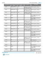
Page 20: ...4 W10 DIFFIO_TX_RX_ B11p High Speed LVDS User I O_4 Note 1 J13 11 USER_LVDS_N6 W5 DIFFIO_TX_RX_ B1n High Speed LVDS User I O_6 Note 1 J13 12 USER_LVDS_N4 W9 DIFFIO_TX_RX_ B11n High Speed LVDS User I O_4 Note 1 J13 13 GND Ground Reference for this group of I Os J13 14 GND Ground Reference for this group of I Os J13 15 USER_LVDS_P7 W3 DIFFIO_TX_RX_ B5p High Speed LVDS User I O_7 Note 1 J13 16 NC Not...

Page 21: ... E16 DIFFIO_RX_T1p High Speed User I O_2 J14 8 USER_IO7 C18 DIFFIO_RX_T7p High Speed User I O_7 J14 9 USER_IO3 C19 DIFFIO_RX_T6n High Speed User I O_3 J14 10 USER_IO8 C17 DIFFIO_RX_T2n High Speed User I O_8 J14 11 GND Ground Reference for this group of I Os J14 12 GND Ground Reference for this group of I Os J14 13 USER_IO4 F16 DIFFIO_RX_T5p High Speed User I O_4 J14 14 USER_IO9 D17 DIFFIO_RX_T2p H...

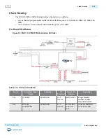
Page 22: ...illators Figure 3 3 MAX 10 10M50 FPGA Evaluation Kit Clocks Table 3 10 On Board Oscillators Source Schematic Signal Name Frequency I O Standard Device Pin Number Application U14 CLK24M 24 000 MHz 1 8 V CMOS MAX 10 M9 Programmable default 24 MHz clock for MAX 10 U14 OV5640_ CLK24MHz 24 000 MHz 3 3 V CMOS 16 POS FFC connector J3 12 Clock for MIPI RX OV5640 module UG 20006 2016 02 29 Clock Circuitry ...

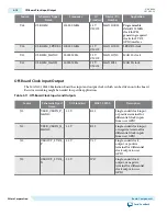
Page 23: ...working might be needed for specific application Table 3 11 Off Board Clock Inputs and Outputs Source Schematic Signal Name I O Standard MAX 10 FPGA Description J12 USER_CLKIN_P_ MAX10 1 2 V K21 Single ended clock input or positive terminal for differential clock inputs from user GPIO J12 USER_CLKIN_N_ MAX10 1 2 V K22 Single ended clock input or negative terminal for differential clock inputs from...

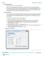
Page 24: ...evice on the board through the JTAG bus The programmable oscillators are connected to the MAX II device through a 2 wire serial bus To run the Clock Control GUI perform the following steps 1 Make sure Quartus II 14 1 or later version is installed 2 Connect the USB cable to the MAX 10M50 FPGA Evaluation Board and power cycle the board 3 Double click the Clock Control GUI application and the interfa...

Page 25: ...r changing frequen cies Note Changing CLK0 of Si5338 will affect the Clock Power GUI Once clock from Port CLK0 is used to drive the MAX II device which is working as a 2 wire serial bus interface connected to Si570 Si5338 and power monitor Components and Interfaces This section describes the evaluation board s ports and optional interface cards relative to the MAX 10 FPGA device HDMI Video Output ...

Page 26: ...HDMI digital video data bus U3 50 HDMI_VIDEO_ DIN10 A13 3 3 V HDMI digital video data bus U3 49 HDMI_VIDEO_ DIN11 B12 3 3 V HDMI digital video data bus U3 48 HDMI_VIDEO_ DIN12 A12 3 3 V HDMI digital video data bus U3 47 HDMI_VIDEO_ DIN13 C12 3 3 V HDMI digital video data bus U3 46 HDMI_VIDEO_ DIN14 A11 3 3 V HDMI digital video data bus U3 45 HDMI_VIDEO_ DIN15 B11 3 3 V HDMI digital video data bus ...

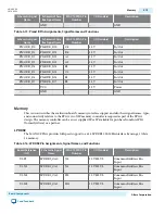
Page 27: ...atible headers which are used to connect low frequency low I O pin count peripheral modules The 12 pin version Pmod connector used in this kit provides 8 I O signal pins The peripheral module interface also encompasses a variant using I2C interface and two or four wire MTE cables The Pmod signals are connected to Bank 8 Table 3 14 Pmod A Pin Assignments Signal Names and Functions Schematic Signal ...

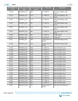
Page 28: ...ace support and also their signal names types and connectivity relative to the FPGA A soft IP memory controller is required as part of the FPGA design The memory controller can be a user supplied IP or IP available for purchase from Intel PSG formerly Altera or a partner LPDDR2 The MAX 10 FPGA provides full speed support to a x16 LPDDR2 200 MHz interface by using a 1Gbit x 16 memory Table 3 16 LPD...

Page 29: ...1 N20 1 2V HSUL Data Bus Byte Lane 0 U2 M7 LPDDR2_DQ2 M20 1 2V HSUL Data Bus Byte Lane 0 U2 M9 LPDDR2_DQ3 M14 1 2V HSUL Data Bus Byte Lane 0 U2 M6 LPDDR2_DQ4 M18 1 2V HSUL Data Bus Byte Lane 0 U2 L7 LPDDR2_DQ5 M15 1 2V HSUL Data Bus Byte Lane 0 U2 L8 LPDDR2_DQ6 L20 1 2V HSUL Data Bus Byte Lane 0 U2 L9 LPDDR2_DQ7 L18 1 2V HSUL Data Bus Byte Lane 0 U2 G9 LPDDR2_DQ8 K20 1 2V HSUL Data Bus Byte Lane 1...

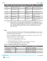
Page 30: ... to provide the designer with a special INI variable Flash The MAX 10 10M50 Evaluation Kit provides a 512 Mb megabit quad SPI flash memory Altera Generic QUAD SPI controller core is used by default to erase read and write quad SPI flash in reference designs of the Board Test System BTS installer If you use the parallel flash loader PFL IP to program the quad SPI flash you need to generate a pof Pr...

Page 31: ...one 1 8V HSTL signal pair and one 2 5V LVCMOS signal pair to support both high speed and low power nodes of one MIPI clock or data lane The control signals RST SCLK and SDATA for LI MIPI USB3 Tester are implemented with both 1 8V and 3 3V options Caution The implemented D PHY resistor values need to be adjusted based on user design Simulation and signal quality measurement is required for optimal ...

Page 32: ... 10 V4 2 5V LVCMOS Differential output data Lane1 high speed negative terminal J1 23 MIPI_TX_DATA_HS_P2 MAX 10 T2 1 8V HSTL Differential output data Lane2 high speed positive terminal J1 22 MIPI_TX_DATA_HS_N2 MAX 10 T1 1 8V HSTL Differential output data Lane2 high speed negative terminal J1 23 MIPI_TX_DATA_LP_P2 MAX 10 AB3 2 5V LVCMOS Differential output data Lane2 high speed positive terminal J1 ...

Page 33: ...1 8V J1 14 MIPI_TX_CMOS_RST_ 3V3 MAX 10 B10 3 3V LVCMOS Reset Power Down 3 3V J1 13 MIPI_TX_CMOS_ SDATA_1V8 MAX 10 N2 1 8V LVCMOS Control Bus Data 1 8V J1 13 MIPI_TX_CMOS_ SDATA_3V3 MAX 10 H12 3 3V LVCMOS Control Bus Data 3 3V J1 12 MIPI_TX_CMOS_SCLK_ 1V8 MAX 10 N3 1 8V LVCMOS Control Bus Clock 1 8V J1 12 MIPI_TX_CMOS_SCLK_ 3V3 MAX 10 J11 3 3V LVCMOS Control Bus Clock 3 3V J1 11 MIPI_TX_CLK24MHz C...

Page 34: ...HSTL signal pair to support low power mode for each MIPI clock or data lane Caution The implemented D PHY resistor values need to be adjusted based on user design Simulation and signal quality measurement is required for optimal resistor values Consult Application Note AN 754 for technical details on implementing the D PHY passive circuits Table 3 20 MIPI CSI 2 Receiver for OV10640 module Pin Assi...

Page 35: ...S_N2 MAX 10 AB19 2 5V LVDS Differential input data Lane2 high speed negative terminal J2 14 OV10640_DATA_ LP_P2 MAX 10 V21 1 2V HSTL Differential input data Lane2 low power positive terminal J2 15 OV10640_DATA_ LP_N2 MAX 10 V22 1 2V HSTL Differential input data Lane2 low power negative terminal J2 17 OV10640_DATA_ HS_P3 MAX 10 AB18 2 5V LVDS Differential input data Lane3 high speed positive termin...

Page 36: ...0640_CMOS_ SCLK MAX 10 P5 1 8V LVCMOS Control Bus Clock J2 26 OV10640_24MHz MAX 10 N5 1 8V LVCMOS 24 MHz Reference Clock Output J2 27 OV10640_GYRO_ INT MAX 10 N9 1 8V LVCMOS Gyroscope Programmable Interrupt J2 28 OV10640_G_RDY MAX 10 R4 1 8V LVCMOS Gyroscope Data Ready J2 31 OV10640_XM_ INT1 MAX 10 R7 1 8V LVCMOS Accelerometer and magnetic sensor interrupt 1 J2 30 OV10640_XM_ INT2 MAX 10 R5 1 8V L...

Page 37: ...h speed positive terminal J3 8 OV5640_DATA_ HS_N1 MAX 10 AB12 2 5V LVDS Differential input data Lane1 high speed negative terminal J3 9 OV5640_DATA_ LP_P1 MAX 10 W19 1 2V HSTL Differential input data Lane1 low power positive terminal J3 8 OV5640_DATA_ LP_N1 MAX 10 W20 1 2V HSTL Differential input data Lane1 low power negative terminal J3 2 OV5640_DATA_ HS_P2 MAX 10 AB11 2 5V LVDS Differential inpu...

Page 38: ...er to wall jack or USB cable to your PC For low power design USB cable connection is suggested and it can easily provide both power and on board USB Blaster connection For high power design DC adapter solution is preferred to ensure device performance The board includes one Jumper J11 for power option selection When use DC power adapter J11 needs to be placed at Position 1 and 2 while for using US...

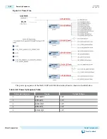
Page 39: ...Board is shown in the table below Table 3 22 Power Up Sequence Table Power Up Sequence Device Output Voltage 1 EP5358HUI 1 8V 2 EP5348UI 1 2V 3 EM5329QI 3 3V 4 EP5384UI 2 5V 5 EN5339QI 1 2V 3 30 Power Up Sequence UG 20006 2016 02 29 Altera Corporation Board Components Send Feedback ...

Page 40: ...tera Corporation All rights reserved ALTERA ARRIA CYCLONE ENPIRION MAX MEGACORE NIOS QUARTUS and STRATIX words and logos are trademarks of Altera Corporation and registered in the U S Patent and Trademark Office and in other countries All other words and logos identified as trademarks or service marks are the property of their respective holders as described at www altera com common legal html Alt...

Page 41: ...Mouser Electronics Authorized Distributor Click to View Pricing Inventory Delivery Lifecycle Information Intel EK 10M50F484 ...

Reviews: