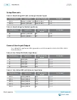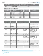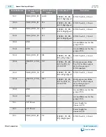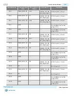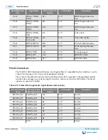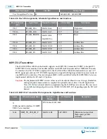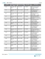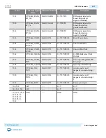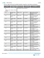
Board Reference
(U2)
Schematic Signal
Name
MAX 10 FPGA Pin
Number
I/O Standard
Description
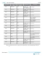
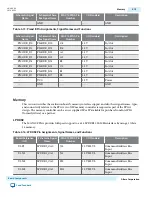
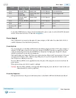
U2.L5
LPDDR2_DQS0n L15
Differential 1.2V
HSUL
Data Strobe N Byte Lane
0
U2.G6
LPDDR2_DQS1
K14
Differential 1.2V
HSUL
Data Strobe Byte P Lane 1
U2.G5
LPDDR2_DQS1n K15
Differential 1.2V
HSUL
Data Strobe Byte N Lane
1
U2.K5
LPDDR2_DM0
N19
1.2V HSUL
Input Data Mask Byte
Lane 0
U2.H5
LPDDR2_DM1
J15
1.2V HSUL
Input Data Mask Byte
Lane 1
U2.D3
LPDDR2_ZQ
/
1.2V HSUL
Output Drive Strength
Calibration
Caution:
When customers start their own design (with unique PCB layout) and still wish to use the
LPDDR2 interface, they should target the 10M50DCF484I6G or 10M50DAF484I6G. For other
MAX 10 parts that support LPDDR2 interfaces (include any 10M16 or higher density MAX 10
device, with dual supply, F256 or higher pin-count, and –i6 speed grade), Quartus access to
these parts requires contacting the local Altera sales person to provide the designer with a
special .INI variable.
Flash
The MAX 10 10M50 Evaluation Kit provides a 512-Mb (megabit) quad SPI flash memory. Altera Generic
QUAD SPI controller core is used by default to erase, read, and write quad SPI flash in reference designs
of the Board Test System (BTS) installer.
If you use the parallel flash loader (PFL) IP to program the quad SPI flash, you need to generate a .pof
(Programmer Object File) to configure the device.
Perform the following steps to generate a .pof file:
1. Create a byte-order Quartus.ini file with the setting:
PGMIO_SWAP_HEX_BYTE_DATA=ON
2. Copy the .ini file to the project root directory and open the project with Quartus
3. Open Convert Programming Files tool to generate the .pof file
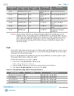
Table 3-17: Default Memory Map of the 512-Mb Quad SPI Flash
Block Description
Size (KB)
Address Range
Board Test System Scratch 512
0x03F8.0000 - 0x03FF.FFFF
User Software
56640
0x0083.0000 - 0x03F7.FFFF
Factory Software
4096
0x0043.0000 - 0x0082.FFFF
Board Information
64
0x0002.0000 - 0x0002.FFFF
UG-20006
2016.02.29
Flash
3-21
Board Components
Altera Corporation
Send Feedback


