background image

Chapter 1: Nios II Hardware Development

1–7

Nios II System Development Flow

May 2011

Altera Corporation

Nios II Hardware Development Tutorial

Hexadecimal (Intel-Format) File (

.hex

)—Contains initialization information for 

on-chip memories. The Nios II SBT for Eclipse generate these initialization files for 
on-chip memories that support initialization of contents. 

Flash memory programming data—Is boot code and other arbitrary data you 
might write to flash memory. The Nios II SBT for Eclipse includes a flash 
programmer, which allows you to write your program to flash memory. The flash 
programmer adds appropriate boot code to allow your program to boot from flash 
memory. You can also use the flash programmer to write arbitrary data to flash 
memory. 

This tutorial focuses on downloading only the 

.elf

 directly to the Nios II system. 

f

For extensive information about developing software for the Nios II processor, refer to 
the 

Nios II Software Developer's Handbook

.

Running and Debugging Software on the Target Board

The Nios II SBT for Eclipse provides complete facilities for downloading software to a 
target board, and running or debugging the program on hardware. The Nios II SBT 
for Eclipse debugger allows you to start and stop the processor, step through code, set 
breakpoints, and analyze variables as the program executes.

f

For information about running and debugging Nios II programs, refer to the tutorial 
in the 

Getting Started with the Graphical User Interface

 chapter of the 

Nios II Software 

Developer’s Handbook

.

Varying the Development Flow

The development flow is not strictly linear. This section describes common variations.

Refining the Software and Hardware

After running software on the target board, you might discover that the Nios II 
system requires higher performance. In this case, you can return to software design 
steps to make improvements to the software algorithm. Alternatively, you can return 
to hardware design steps to add acceleration logic. If the system performs multiple 
mutually exclusive tasks, you might even decide to use two (or more) Nios II 
processors that divide the workload and improve the performance of each individual 
processor.

Iteratively Creating a Nios II System

A common technique for building a complex Nios II system is to start with a simpler 
Qsys system, and iteratively add to it. At each iteration, you can verify that the system 
performs as expected. You might choose to verify the fundamental components of a 
system, such as the processor, memory, and communication channels, before adding 
more complex components. When developing a custom component or a custom 
instruction, first integrate the custom logic into a minimal system to verify that it 
works as expected; later you can integrate the custom logic into a more complex 
system.

Summary of Contents for Nios II

Page 1: ...101 Innovation Drive San Jose CA 95134 www altera com TU N2HWDV 4 0 Tutorial Nios II Hardware Development Subscribe Nios II Hardware Development Tutorial ...

Page 2: ...l html Altera warrants performance of its semiconductor products to current specifications in accordance with Altera s standard warranty but reserves the right to make changes to any products and services at any time without notice Altera assumes no responsibility or liability arising out of the application or use of any information product or service described herein except as expressly agreed to...

Page 3: ...Open the Example Project 1 9 Create a New Qsys System 1 10 Define the System in Qsys 1 11 Specify Target FPGA and Clock Settings 1 11 Add the On Chip Memory 1 12 Add the Nios II Processor Core 1 14 Add the JTAG UART 1 17 Add the Interval Timer 1 18 Add the System ID Peripheral 1 19 Add the PIO 1 20 Specify Base Addresses and Interrupt Request Priorities 1 22 Generate the Qsys System 1 23 Integrate...

Page 4: ...iv Contents Nios II Hardware Development Tutorial May 2011 Altera Corporation ...

Page 5: ...ign steps Where appropriate the tutorial refers you to further documentation for greater detail f If you are interested only in software development for the Nios II processor refer to the tutorial in the Getting Started with the Graphical User Interface chapter of the Nios II Software Developer s Handbook When you complete this tutorial you will understand the Nios II system development flow and y...

Page 6: ...nd Hardware Requirements This tutorial requires you to have the following software Altera Quartus II software version 11 0 or later The software must be installed on a Windows or Linux computer that meets the Quartus II minimum requirements f For system requirements and installation instructions refer to Altera Software Installation and Licensing Nios II EDS version 11 0 or later Design files for ...

Page 7: ... an Altera USB Blaster download cable revision B or higher or a USB connection with USB Blaster circuitry embedded on the board 1 To complete this tutorial you must refer to the documentation for your board that describes clock frequencies and pinouts For Altera development boards you can find this information in the associated reference manual f For information about Altera development kits and d...

Page 8: ...gn flow The design steps in this tutorial focus on hardware development and provide only a simple introduction to software development f After completing this tutorial refer to the Nios II Software Developer s Handbook especially the tutorial in the Getting Started with the Graphical User Interface chapter for more information about the software development process The handbook is a complete refer...

Page 9: ...e teams Defining and Generating the System in Qsys After analyzing the system hardware requirements you use Qsys to specify the Nios II processor core s memory and other components your system requires Qsys automatically generates the interconnect logic to integrate the components in the hardware system You can select from a list of standard processor cores and components provided with the Nios II...

Page 10: ...er After configuration the FPGA behaves as specified by the hardware design which in this case is a Nios II processor system f For further information about using the Quartus II software refer to Introduction to the Quartus II Software the Quartus II Handbook and the Quartus II Software Interactive Tutorial in the Training Courses section of the Altera website Developing Software with the Nios II ...

Page 11: ...e variables as the program executes f For information about running and debugging Nios II programs refer to the tutorial in the Getting Started with the Graphical User Interface chapter of the Nios II Software Developer s Handbook Varying the Development Flow The development flow is not strictly linear This section describes common variations Refining the Software and Hardware After running softwa...

Page 12: ...omponents provided with the Nios II EDS the easiest way to verify functionality is to download the hardware and software directly to a development board f For information about performing hardware simulation for Nios II system refer to Simulating Nios II Embedded Processor Designs Creating the Design Example This section guides you through the Nios II development flow to create a working design ex...

Page 13: ...Nios II system that works on any board with an Altera FPGA The entire system must use only on chip resources and not rely on the target board The design should conserve on chip logic and memory resources so it can fit in a wide range of target FPGAs These goals lead to the following design decisions The Nios II system uses only the following inputs and outputs One clock input which can be any cons...

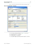
Page 14: ...s2_project qpf and click Open The project opens 5 To display the Block Diagram File bdf nios2_quartus2_project bdf Figure 1 3 perform the following steps a On the File menu click Open The Open dialog box appears b Browse to the design files directory c Select nios2_quartus2_project bdf and click Open Figure 1 3 shows the nios2_quartus2_project bdf file The bdf contains an input pin for the clock i...

Page 15: ...d the stderr character stream In this section you perform the following steps 1 Specify target FPGA and clock settings 2 Add the Nios II core on chip memory and other components 3 Specify base addresses and interrupt request IRQ priorities 4 Generate the Qsys system The Qsys design process does not need to be linear The design steps in this tutorial are presented in the most straightforward order ...

Page 16: ... clk_0 is the default clock input name for the Qsys system The frequency you specify for clk_0 must match the oscillator that drives the FPGA 4 Type the clock frequency and press Enter Next you begin to add hardware components to the Qsys system As you add each component you configure it appropriately to match the design specifications Add the On Chip Memory Processor systems require at least one ...

Page 17: ...tents tab An instance of the on chip memory appears in the system contents table 1 For more information about on chip memory you can click Documentation in the On Chip Memory RAM or ROM parameter editor This documentation feature is available in the parameter editor for each component 7 In the Name column of the system contents table right click the on chip memory and click Rename 8 Type onchip_me...

Page 18: ...re 1 6 shows the GUI 3 Under Select a Nios II core select Nios II s 4 In the Hardware multiplication type list select None 5 Turn off Hardware divide 6 Click Finish You return to the Qsys System Contents tab and an instance of the Nios II core appears in the system contents table Ignore the exception and reset vector error messages You resolve these errors in steps 13 and 14 7 In the Name column r...

Page 19: ...e Core Nios II tab of the Nios II Processor parameter editor 15 Click the Caches and Memory Interfaces tab Figure 1 7 shows the GUI 16 In the Instruction cache list select 2 Kbytes 17 In the Burst transfers list select Disable 18 In the Number of tightly coupled instruction master port s list select None Figure 1 6 Nios II Parameter Editor Core Nios II Tab ...

Page 20: ...JTAG Debug Module or Custom Instruction tabs 19 Click Finish You return to the Qsys System Contents tab f For more information about configuring the Nios II core refer to the Instantiating the Nios II Processor in Qsys chapter of the Nios II Processor Reference Handbook f For more information about connecting memory to Nios II systems refer to the System Design with Qsys section of Volume 1 Design...

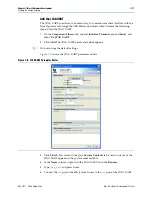
Page 21: ...t Library tab expand Interface Protocols expand Serial and then click JTAG UART 2 Click Add The JTAG UART parameter editor appears 1 Do not change the default settings Figure 1 8 shows the JTAG UART parameter editor 3 Click Finish You return to the Qsys System Contents tab and an instance of the JTAG UART appears in the system contents table 4 In the Name column right click the JTAG UART and click...

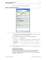
Page 22: ...t send instructions to the Nios II processor f For more information about the JTAG UART refer to the JTAG UART Core chapter in the Embedded Peripherals IP User Guide Add the Interval Timer Most control systems use a timer component to enable precise calculation of time To provide a periodic system clock tick the Nios II HAL requires a timer Perform the following steps to add the timer 1 On the Com...

Page 23: ... to the clk port of the interval timer 8 Connect the clk_reset port of the clk_0 clock source to the reset port of the interval timer 9 Connect the data_master port of the Nios II processor to the s1 port of the interval timer f For more information about the timer refer to the Timer Core chapter in the Embedded Peripherals IP User Guide Add the System ID Peripheral The system ID peripheral safegu...

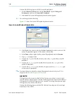
Page 24: ...press Enter 6 Connect the clk port of the clk_0 clock source to the clk port of the system ID peripheral 7 Connect the clk_reset port of the clk_0 clock source to the reset port of the system ID peripheral 8 Connect the data_master port of the Nios II processor to the control_slave port of the system ID peripheral f For more information about the system ID peripheral refer to the System ID Core ch...

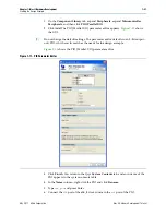
Page 25: ...the GUI 1 Do not change the default settings The parameter editor defaults to an 8 bit output only PIO which exactly matches the needs for the design example Figure 1 11 shows the PIO Parallel I O parameter editor 3 Click Finish You return to the Qsys System Contents tab and an instance of the PIO appears in the system contents table 4 In the Name column right click the PIO and click Rename 5 Type...

Page 26: ...es Do not worry about choosing address values that are easy to remember Address values that differentiate components with only a one bit address difference produce more efficient hardware Do not worry about compacting all base addresses into the smallest possible address range because this can create less efficient hardware Qsys does not attempt to align separate memory components in a contiguous ...

Page 27: ... with the complete system Generate the Qsys System You are now ready to generate the Qsys system Perform the following steps 1 Click the Generation tab 2 Select None in both the Create simulation model and Create testbench Qsys system lists Because this tutorial does not cover the hardware simulation flow you can select these settings to shorten generation time 3 Click Generate The Save changes di...

Page 28: ...Qsys and return to the Quartus II software Congratulations You have finished creating the Nios II processor system You are ready to integrate the system into the Quartus II hardware project and use the Nios II SBT for Eclipse to develop software f For more information about generating systems with Qsys refer to the System Design with Qsys section of Volume 1 Design and Synthesis of the Quartus II ...

Page 29: ...ct For example if you were using Verilog HDL for design entry you would instantiate the Verilog module first_nios2_system defined in the file first_nios2_system v To instantiate the system module in the bdf perform the following steps 1 Double click in the empty space to the right of the input and output wires The Symbol dialog box appears 2 Under Libraries expand Project 3 Click first_nios2_syste...

Page 30: ...ystem synthesis first_nios2_system qip and click Open to select the file 6 Click Add to include first_nios2_system qip in the project 7 Click OK to close the Settings dialog box Assign FPGA Device and Pin Locations In this section you assign a specific target device and then assign FPGA pin locations to match the pinouts of your board 1 You must know the pin layout for the board to complete this s...

Page 31: ...s do so 5 Click OK to accept the device assignment Figure 1 15 shows an example of the Device dialog box To assign the FPGA pin locations perform the following steps 1 On the Processing menu point to Start and click Start Analysis Elaboration to prepare for assigning pin locations The analysis starts by displaying a data not available message and can take several minutes A confirmation message box...

Page 32: ...double click in the I O Standard cell to access a list of available I O standards 8 Select the appropriate I O standard that connects to the oscillator on the board 9 If you connected the LED pins in the board design schematic repeat steps 4 to 8 for each of the LED output pins LEDG 0 LEDG 1 LEDG 2 LEDG 3 LEDG 4 LEDG 5 LEDG 6 LEDG 7 to assign appropriate pin locations 10 On the File menu click Clo...

Page 33: ... to account for the board design Consult with the maker of the board for specific contention information 15 Click OK to close the Device and Pin Options dialog box 16 Click OK to close the Device dialog box f For more information about making assignments in the Quartus II software refer to the Volume 2 Design Implementation and Optimization of the Quartus II Handbook Compile the Quartus II Project...

Page 34: ...create_clock command create_clock name sopc_clk period 20 get_ports PLD_CLOCKINPUT 5 Change the period setting from 20 to the clock period 1 frequency in nanoseconds of the oscillator driving the clock pin 6 On the File menu click Save 7 On the Assignments menu click Settings The Settings dialog box appears 8 Under Category click TimeQuest Timing Analyzer Figure 1 18 shows the TimeQuest Timing Ana...

Page 35: ...rtus II assignments to optimize fitting or reduce the oscillator frequency driving the FPGA f For more information about meeting timing requirements in the Quartus II software refer to the Volume 1 Design and Synthesis of the Quartus II Handbook Congratulations You have finished integrating the Nios II system into the Quartus II project You are ready to download the sof to the target board Downloa...

Page 36: ...sing the Nios II SBT for Eclipse to develop programs refer to the Getting Started with the Graphical User Interface chapter of the Nios II Software Developer s Handbook In this section you perform the following actions Create new Nios II C C application and BSP projects Compile the projects To perform this section you must have the sopcinfo file you created in Define the System in Qsys on page 1 1...

Page 37: ...st_nios2_system sopcinfo and click Open You return to the Nios II Application and BSP from Template wizard showing current information for the SOPC Information File name and CPU name fields 7 In the Project name box type count_binary 8 In the Templates list select Count Binary 9 Click Finish The Nios II SBT for Eclipse creates and displays the following new projects in the Project Explorer view ty...

Page 38: ...k Properties The Properties for count_binary_bsp dialog box appears 2 Click the Nios II BSP Properties page The Nios II BSP Properties page contains basic software build settings Figure 1 21 shows the GUI 1 Though not needed for this tutorial note the BSP Editor button in the lower right corner of the dialog box You use the Nios II BSP Editor to access advanced BSP settings 3 Adjust the following ...

Page 39: ...rs verify that Project name and ELF file name contain relevant data then click Run When the target hardware starts running the program the Nios II Console view displays character I O output Figure 1 22 shows the output If you connected LEDs to the Nios II system in Integrate the Qsys System into the Quartus II Project on page 1 24 then the LEDs blink in a binary counting pattern 2 Click the Termin...

Page 40: ...ce for developing software for the Nios II processor The software development tutorial in the Getting Started with the Graphical User Interface chapter of the Nios II Software Developer s Handbook This tutorial teaches in detail how to use the Nios II SBT for Eclipse to develop run and debug new Nios II C C application projects Nios II Processor Reference Handbook This handbook provides complete r...

Page 41: ... Added altera components project information Minor text changes May 2007 2 4 Updated to describe new SOPC Builder MegaWizard design flow Added OpenCore Plus information March 2007 2 3 Maintenance release for v7 0 software November 2006 2 2 Minor text changes May 2006 2 1 Revised and simplified the tutorial flow May 2005 2 0 Revised the introductory information December 2004 1 1 Updated for the Nio...

Page 42: ...urier type Indicates signal port register bit block and primitive names For example data1 tdi and input The suffix n denotes an active low signal For example resetn Indicates command line commands and anything that must be typed exactly as it appears For example c qdesigns tutorial chiptrip gdf Also indicates sections of an actual file such as a Report File references to parts of files for example...

Reviews: