background image


40 

5

5

.

.

4

4


R

R

e

e

s

s

t

t

o

o

r

r

i

i

n

n

g

g


t

t

h

h

e

e


F

F

a

a

c

c

t

t

o

o

r

r

y

y


I

I

m

m

a

a

g

g

e

e


This section describes some details about the operation of restoring the Application Selector factory 
image. 

Combining factory recovery binary files


In  the  factory  settings,  you  need  to  program  Application  Selector  binary  files  to  EPCS.  Before 
programming,  you  should  combine  application  selector  software  binary  file  and  hardware  binary 
file together by executing the instructions below: 


Copy both the tPad_Selector.sof and tPad_Selector.elf files into a common directory relying on 
your choice. This directory is where you will convert the files 


On your host PC, launch a Nios II Command Shell from 

Start

 ->

Programs

 -> 

Altera

 -> 

Nios 

II <version #> EDS

 -> 

Nios II Command Shell


From the command shell navigate to where your SOF file is located and create your hardware 
binary file using the following command commands listed below 


Convert tPad_Selector.sof file into tPad_Selector

_HW

.flash file 

sof2flash    --epcs –input=tPad_Selector.sof    --output= tPad_Selector_HW.flash 


Convert .flash file into .bin file 

nios2-elf-objcopy –I srec –O binary tPad_Selector

_HW

.flash tPad_Selector

_HW

.bin 


From the command shell navigate to where your ELF file is located and create your software 
bin image using the following command commands listed below 


Convert tPad_Selector.elf    into tPad_Selector

_SW

.flash 

elf2flash –epcs    --after=tPad_Selector_HW.flash --input=tPad_Selector.elf 
--output=tPad_Selector

_SW

.flash 


Convert tPad_Selector

_SW

.flash into tPad_Selector

_SW

.bin 

nios2-elf-objcopy –I srec –O binary tPad_Selector

_SW

.flash tPad_Selector_SW.bin 


Combine tPad_Selector

_HW

.bin and tPad_Selector_SW.bin using the following command 

cat tPad_Selector

_HW

.bin    tPad_Selector

_SW

.bin > tPad_Selector.bin 


The generated tPad_Selector.bin is our target binary file 


Summary of Contents for tPad DE2-115

Page 1: ...1 ...

Page 2: ...tal Image Sensor Module 15 Chapter 4 tPad Demonstrations 17 4 1 System Requirements 17 4 2 Factory Configuration 17 4 3 tPad Starter Demonstration 18 4 4 tPad Picture Viewer 22 4 5 Video and Image Processing 25 4 6 tPad Camera Application 28 4 7 Video and Image Processing for Camera 31 Chapter 5 Application Selector 36 5 1 Ready to Run SD Card Demos 36 5 2 Running the Application Selector 37 5 3 A...

Page 3: ... with an FPGA hardware reference design including several Ready to Run demonstration applications stored on the provided SD Card Software developers can use these reference designs as their platform to quickly architect develop and build complex embedded systems By simply scrolling through the demo of your choice on the LCD multimedia color touch panel you can evaluate numerous processor system de...

Page 4: ... blocks o 3 888 Kbits embedded memory o 4 PLLs Configuration o On board USB Blaster circuitry o JTAG and AS mode configuration supported o EPCS64 serial configuration device Memory Devices o 128MB SDRAM o 2MB SRAM o 8MB Flash with 8 bit mode o 32Kbit EEPROM Switches and Indicators o 18 switches and 4 push buttons o 18 red and 9 green LEDs o Eight 7 segment displays ...

Page 5: ...zanine Card HSMC o Configurable I O standards voltage levels 3 3 2 5 1 8 1 5V USB Type A and B o Provide host and device controller compliant with USB 2 0 o Support data transfer at full speed and low speed o PC driver available 40 pin Expansion Port o Configurable I O standards voltage levels 3 3 2 5 1 8 1 5V VGA out Connector o VGA DAC high speed triple DACs DB9 Serial Connector o RS232 port wit...

Page 6: ... dot Dot pitch 0 0675 W x 0 2025 H mm Active area 162 0 W x 121 5 H mm Module size 183 0 W x 141 0 H x 7 2 D mm Surface treatment Anti Glare Color arrangement RGB stripe Interface Digital 5 Megapixel digital image sensor module Superior low light performance High frame rate Low dark current Global reset release which starts the exposure of all rows simultaneously Bulb exposure mode for arbitrary e...

Page 7: ...solution 12 bit Responsivity 1 4V lux sec 550nm Pixel dynamic range 70 1dB SNRMAX 38 1dB Supply Voltage Power 3 3V I O 1 7V 3 1V Note for more detailed information of the LCD touch panel and CMOS sensor module please refer to their datasheets respectively 1 1 1 1 A Ab bo ou ut t t th he e K Ki it t The kit contains all users needed to run the demonstrations and develop custom designs as shown in F...

Page 8: ...e 1 2 tPad kit package contents 1 1 2 2 G Ge et tt ti in ng g H He el lp p Here is information of how to get help if you encounter any problem Terasic Technologies Tel 886 3 550 8800 Email support terasic com ...

Page 9: ...agram and components 2 2 1 1 L La ay yo ou ut t a an nd d C Co om mp po on ne en nt ts s The picture of the tPad is shown in Figure 2 1 and Figure 2 2 It depicts the layout of the board and indicates the locations of the connectors and key components Figure 2 1 tPad PCB and component diagram top view ...

Page 10: ...a am m o of f t th he e t tP Pa ad d Figure 2 3 gives the block diagram of the tPad board To provide maximum flexibility for the user all connections are made through the Cyclone IV E FPGA device Thus the user can configure the FPGA to implement any system design Figure 2 3 Block Diagram of tPad ...

Page 11: ...to the board the configuration information will be lost when the power is turned off 2 AS programming In this method called Active Serial programming the configuration bit stream is downloaded into the Altera EPCS64 serial configuration device It provides non volatile storage of the bit stream so that the information is retained even when the power supply to the tPad board is turned off When the b...

Page 12: ... E FPGA perform the following steps Ensure that power is applied to the tPad board Configure the JTAG programming circuit by setting the RUN PROG slide switch SW19 to the RUN position See Figure 3 4 Connect the supplied USB cable to the USB Blaster port on the tPad board The FPGA can now be programmed by using the Quartus II Programmer module to select a configuration bit stream file with the sof ...

Page 13: ...SB cable to the USB Blaster port on the tPad board Configure the JTAG programming circuit by setting the RUN PROG slide switch SW19 to the PROG position The EPCS64 chip can now be programmed by using the Quartus II Programmer module to select a configuration bit stream file with the pof filename extension Once the programming operation is finished set the RUN PROG slide switch back to the RUN posi...

Page 14: ...roduction The bus controller provides level shifting functionality from 2 5V HSMC to 3 3V domains Block Diagram of the Bus Controller Figure 3 6 gives the block diagram of the connection setup from the HSMC connector to the bus controller on the Max II EPM240 to the touch screen module To provide maximum flexibility for the user all connections are established through the HSMC connector Thus the u...

Page 15: ...lock signals must act according to the timing specification of the LCD touch panel as shown in Table 3 1 Table 3 2 gives the pin assignment information of the LCD touch panel Table 3 1 LCD timing specifications Parameter Symbol Values Unit Min Typ Max CLK Frequency FCPH 39 79 MHz CLK Period FCPH 25 13 Ns CLK Pulse Duty FCWH 40 50 60 DE Period FDEH TDEL 1000 1056 TCPH DE Pulse Width FDH 800 TCPH DE...

Page 16: ...N_U25 AD7843 serial interface data in 2 5V TOUCH _CS_N PIN_T26 AD7843 serial interface chip select input 2 5V TOUCH _DCLK PIN_T25 AD7843 interface clock 2 5V 3 3 4 4 U Us si in ng g 5 5 M Me eg ga ap pi ix xe el l D Di ig gi it ta al l I Im ma ag ge e S Se en ns so or r M Mo od du ul le e The tPad is equipped with a 5 Megapixel digital image sensor module that provides an active imaging array of 2...

Page 17: ...D9 PIN_L24 Pixel data bit 9 2 5V CAMERA_ D10 PIN_M25 Pixel data bit 10 2 5V CAMERA_ D11 PIN_M26 Pixel data bit 11 2 5V CAMERA_ STROBE PIN_G28 Snapshot strobe 2 5V CAMERA_ LVAL PIN_K27 Line valid 2 5V CAMERA_ FVAL PIN_K28 Frame valid 2 5V CAMERA_ RESET_N PIN_M28 Image sensor reset 2 5V CAMERA_ SCLK PIN_K22 Serial clock 2 5V CAMERA_ TRIGGER PIN_H23 Snapshot trigger 2 5V CAMERA_ SDATA PIN_H24 Serial ...

Page 18: ...arted with Altera s DE2 115 Board tut_initialDE2 115 pdf which is available on the DE2 115 system CD Copy the entire demonstrations folder from the tPad system CD to your host computer 4 4 2 2 F Fa ac ct to or ry y C Co on nf fi ig gu ur ra at ti io on n The tPad development kit comes preconfigured with a default utility that boots up on power on and allows users to quickly select load and run dif...

Page 19: ...ator can be treated as an upgrade version of the LCD test program The software successively generates different color patterns after a fixed time delay Users could use it to quickly investigate any flaw of the LCD Figure 4 2 shows the hardware system block diagram of this demonstration The system is clocked by an external 50MHz Oscillator Through the internal PLL module the generated 100MHz clock ...

Page 20: ...emonstration The touch panel s SPI HAL block responds to the bottom hardware requests and interface to upper layers The SGDMA HAL allocates required frame descriptor buffers to specified memory address and is responsible of handling frame buffer update issue Figure 4 3 Software stack of the tPad Starter demonstration ...

Page 21: ...us II and Nios II are installed on your PC Power on the DE2 115 board Connect USB Blaster to the DE2 115 board and install USB Blaster driver if necessary Execute the demo batch file tPad_Starter bat under the batch file folder tPad_Starter demo_batch After Nios II program is downloaded and executed successfully a prompt message will be displayed in nios2 terminal From on the touch panel tap any i...

Page 22: ...21 Figure 4 4 Main interface of the tPad Starter demonstration Figure 4 5 The tPad Starter Touch sub item ...

Page 23: ...RAM The tPad will show the image the buffer being displayed points to When users touch the LCD Touch Panel it will proceed to display the next buffered image until there is no filled buffer and enter the Loading phase Figure 4 7 shows the block diagram of this demonstration The Nios II CPU here takes a key roll in the demonstration It is responsible of decoding the JPEG images and coordinates the ...

Page 24: ...batch file includes the following files Batch File tPad_Picture_Viewer bat tPad_Picture_Viewer _bashrc FPGA Configure File tPad_Picture_Viewer sof Nios II Program tPad_Picture_Viewer elf Demonstration Setup Format your SD Card into FAT16 format Place the jpg image files to the jpg subdirectory of the SD Card For best display result the image should have a resolution of 800x600 or the multiple of t...

Page 25: ...stration Table 4 1 shows the instructions for running the demonstration Figure 4 8 tPad picture viewer demonstration Table 4 1 Touch panel displayed information Display information Implication Press the play button to display the next buffered image Indicates the loading progress Note execute the tPAD_Picture_Viewer bat under tPAD_Picture_Viewer demo_batch will automatically download the sof and e...

Page 26: ...e FIR filter on an image data stream to smooth or sharpen images Alpha Blending Mixer Mixes and blends multiple image streams useful for implementing text overlay and picture in picture mixing Scaler A sophisticated polyphase scaler that allows custom scaling and real time updates of both the image sizes and the scaling coefficients Deinterlacer Converts interlaced video formats to progressive vid...

Page 27: ...deo system is implemented using the SOPC Builder system level design tool This abstracted design tool provides an easy path to system integration of the video processing data path with a NTSC or PAL video input VGA output Nios II processor for configuration and control The Video and Image Processing Suite MegaCore functions have common open Avalon ST data interfaces and Avalon Memory Mapped Avalon...

Page 28: ...Pad board The DVD player has to be configured to provide NTSC output or PAL output Connect the VGA output of the tPad board to a VGA monitor both LCD and CRT type of monitors should work Load the bit stream into FPGA note Run the Nios II and choose tPad_VIP Software as the workspace Click on the Run button note Press and drag the video frame box will result in scaling the playing window to any siz...

Page 29: ... reference design using the 5 Megapixel CMOS sensor and 8 inch LCD modules on the tPad The CMOS sensor module sends the raw image data to FPGA on DE2 115 Board the FPGA on the board is handling image processing part and converts the data to RGB format to display on the LCD module The I2C Sensor Configuration module is used to configure the CMOS sensor module Figure 4 12 shows the block diagram of ...

Page 30: ...e RAW2RGB block After that the Multi Port SDRAM Controller acquires and writes the RGB data streams to the SDRAM which performs as a frame buffer The Multi Port SDRAM Controller has two write ports and read ports also with 16 bit data width each The writing clock is the same as CMOS sensor pix clock and the reading clock is provided by the LCD Controller which is 40MHz Finally the LCD controller f...

Page 31: ...t of the photo you can press KEY 3 again to switch back to FREE RUN mode and you should be able to see whatever the camera captures on the LCD display User can use the SW 0 and KEY 1 to set the exposure time for brightness adjustment of the image captured When SW 0 is set to Off the brightness of image will be increased as KEY 1 is pressed longer If SW 0 is set to On the brightness of image will b...

Page 32: ... si in ng g f fo or r C Ca am me er ra a The Video and Image Processing VIP for Camera Example Design demonstrates dynamic scaling and clipping of a standard definition video stream in RGB format and picture in picture mixing with a background layer The video stream is output in high definition resolution 800 600 on the HSMC LTC daughter card part of the tPad The example design demonstrates a fram...

Page 33: ...ovided The video system is implemented using the SOPC Builder system level design tool This abstracted design tool provides an easy path to system integration of the video processing data path with a NTSC or PAL video input VGA output Nios II processor for configuration and control The Video and Image Processing Suite MegaCore functions have common open Avalon ST data interfaces and Avalon Memory ...

Page 34: ...nts Demonstration Source Code Project directory tPad_VIP_Camera Bit stream used tPad_VIP_Camera sof Nios II Workspace tPad_VIP_Camera Software Demonstration Batch File Demo Batch File Folder tPad_VIP_Camera demo_batch The demo batch file includes the following files ...

Page 35: ... the DE2 115 board to reset the circuit Press KEY 2 to stop run you can press KEY 3 again to switch back to FREE RUN mode and you should be able to see whatever the camera captures on the VGA display User can use SW 17 to mirror image of the line However remember to press KEY 0 after toggle SW 17 Press and drag the video frame box will result in scaling the playing window to any size as shown in F...

Page 36: ...35 Figure 4 15 Setup for the tPad_VIP_Camera demonstration ...

Page 37: ...demos in your SD Card root directory as well as in the System CD under tPad_Factory_Recovery Application_Selector folder Figure 5 1 shows the photograph of the application selector main interface Figure 5 1 Application selector main interface Also you can easily convert your own applications to be loadable by the application selector For more information see Creating Your Own Loadable Applications...

Page 38: ...e names are supported The Nios II CPU access the SD Card through an SD Card SPI controller Application Files Each loadable application consists of two binary files all stored on the SD Card The first binary file represents the software portion of the example and must be derived from an ELF file as described in the section of this document titled Creating Your Own Loadable Applications This binary ...

Page 39: ...cations It is easy to convert your own Nios II design into an application which is loadable by the Application Selector utility All you need is a hardware image a SOF file and a software image which runs on that hardware a Nios II ELF file The only restrictions are The hardware designs must contain a CFI Flash controller 1 If the SOF file contains a Nios II CPU then its reset address should be set...

Page 40: ...n does not contain a Nios II processor or you store your software code within the on chip memory and use the hex initialization file 2 If you would like to use other memories such as SRAM or SDRAM as the program memory you may need to perform two steps to convert your elf file into bin file to make the software properly run on tPad The commands seem to look like this elf2flash base flash_base_addr...

Page 41: ...SOF file is located and create your hardware binary file using the following command commands listed below Convert tPad_Selector sof file into tPad_Selector_HW flash file sof2flash epcs input tPad_Selector sof output tPad_Selector_HW flash Convert flash file into bin file nios2 elf objcopy I srec O binary tPad_Selector_HW flash tPad_Selector_HW bin From the command shell navigate to where your ELF...

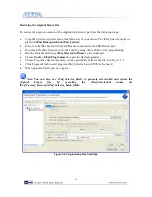
Page 42: ...sing either JTAG or AS programming Run the Nios II and choose tPad_Selector Software as the workspace Choose Tools Flash Programmer to open the flash programmer Choose Program a file into memory choose your tPad_Selector bin file See Figure 5 2 Click Program Flash to start program tPad_Selector bin to EPCS in the board When program finish power on again Note You can also use tPad_Selector_batch to...

Page 43: ... y Version Change Log V1 0 Initial Version Preliminary V1 0 1 Kit content image updated V1 0 2 Descriptions of the camera demonstration s mirror mode added 6 6 2 2 C Co op py yr ri ig gh ht t S St ta at te em me en nt t Copyright 2010 Terasic Technologies All rights reserved ...

Reviews: