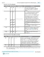
Table 16-17: ATX Tuning Registers
ATX Addr
Bits
R/W
Register Name
Description
7’h30
[9:0] RW
logical channel number
The logical channel number. The
Transceiver Reconfiguration Controller
maps the logical address to the physical
address.
7’h32
[9]
R
control and status
Error
. When asserted, indicates an invalid
channel or address. This bit is asserted
after a write operation if the selected
logical channel number
selects a logical
channel interface that is not connected to
an ATX PLL. It is also be asserted if the
tuning algorithm failed to converge on a
working setting after a manual calibration.
[8]
R
Busy
. When asserted, indicates that a
reconfiguration operation is in progress.
[1]
W
Read
. Writing a 1 to this bit triggers a read
operation.
[0]
W
Write
. Writing a 1 to this bit triggers a
write operation.
7’h33
[3:0] RW
atx_offset
Specifies the 4-bit register address used for
indirect accesses on the reconfiguration
bus. Refer to
Table 16-18
for offsets and
values.
7’h34
[15:0] RW
data
Reconfiguration data for the transceiver
PHY registers.
Table 16-18: ATX PLL Tuning Offsets and Values
Offset
Bits
R/W
Register Name
Description
0x0
[0]
RW
Control
Writing a 1 to this bit triggers ATX PLL calibration. This
register self-clears. Unused bits of this register must be
set to 0. The
tx_cal_busy
signal is asserted at initial
runtime or if you reset the reconfiguration controller. It
is not asserted if you manually re-trigger the ATX PLL
calibration process. Writing a 1 to this bit will not
trigger ATX PLL calibration if the PLL is already locked.
0x1
[1]
RW
Writing a 1 to this bit triggers the ATX PLL calibration
even if the PLL is already locked.
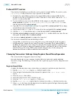
Refer to Changing Transceiver Settings Using Register-Based Reconfiguration for the procedures you can
use to control ATX tuning.
UG-01080
2015.01.19
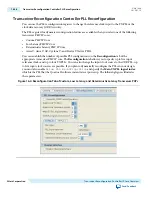
Transceiver Reconfiguration Controller ATX PLL Calibration Registers
16-27
Transceiver Reconfiguration Controller IP Core Overview
Altera Corporation
Send Feedback


