UG-293
AD9643/AD9613/AD6649/AD6643 User Guide
Rev. A | Page 8 of 26
2.
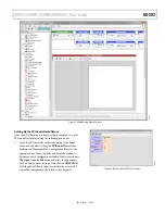
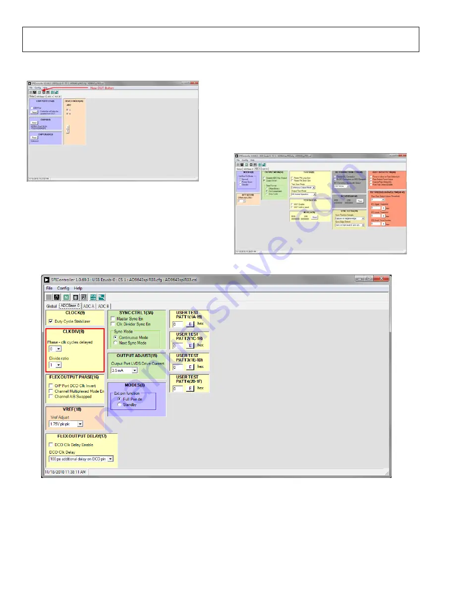
Click the
New DUT
button in the
SPIController
window
(see Figure 9).
0
9940
-0
09
Figure 9. SPI Controller, New DUT Button
3.
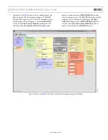
In the
ADCBase 0
tab of the
SPIController
window, find
the
CLK DIV(B)
section (see Figure 11). If using the clock
divider, use the drop-down box to select the correct clock
divide ratio, if necessary. See the appropriate device data sheet;
the
AN-878 Application Note
,
High Speed ADC SPI Control
Software
; and the
AN-877 Application Note
,
Interfacing to
High Speed ADCs via SPI
, for additional information.
4.
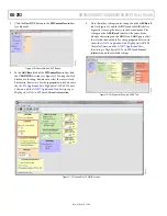
Note that other settings can be changed on the
ADCBase 0
tab (see Figure 11) and the
ADC A
and
ADC B
tabs (see
Figure 10) to set up the device in the desired mode. The
settings on the
ADCBase 0
tab affect the entire device,
whereas the settings on the
ADC A
and
ADC
pages affect
the selected channel only. See the appropriate device data
sheet; the
AN-878 Application Note
,
High Speed ADC SPI
Control Software
; and the
AN-877 Application Note
,
Interfacing to High Speed ADCs via SPI
, for additional
information on the available settings.
0
994
0-
0
1
1
Figure 10. SPI Controller, Example ADC A Tab
0
994
0-
01
0
Figure 11. SPI Controller, CLK DIV(B) Section


