background image


Rev 05 Jun 2013 16:37 | Page 6

Power

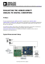
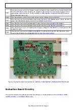
Plug the switching power supply into a wall outlet rated at 100 V ac to 240 V ac, 47 Hz to 63 Hz.
Connect the DC output connector to P101 on the evaluation board.

Analog Input

The analog input on the evaluation board is set up for a double balun-coupled analog input with a 50
Ω impedance. The default analog input configuration supports analog input frequencies of up to ~400
MHz. For additional information on recommended input networks, see the 

AD9683

 and 

AD6677

 data

sheets.

Optionally, the 

AD9683

 and 

AD6677

 analog input can be configured to use the 

ADL5202

 digitally

controlled, variable gain wide bandwidth amplifier. The 

ADL5202

 is included on the evaluation board

at U401. The path into and out of the 

ADL5202

 can be configured many different ways depending on

the application; therefore, several of the components in the input and output path are left
unpopulated. See the 

ADL5202

 data sheet for additional information on this part and for configuring

the inputs and outputs.

In order to connect the active path using the 

ADL5202

 a few resistors need to be changed. First,

remove C305 and C306. Then populate R311 and R312. These changes disconnect the passive input
and connect the output of the 

ADL5202

 to the analog inputs of the 

AD9683

 and 

AD6677

. Next, place

the desired filter components at the output of the 

ADL5202

. As mentioned, these are not populated

by default since there are many different possibilities. J404 must also be populated so that the input
of the 

ADL5202

 can be driven with an external signal source.

Clock

Nyquist Clock

The default clock input circuit connects to the Nyquist clock input of the 

AD9683

 and 

AD6677

. The

clock is derived from a simple transformer-coupled circuit using a high bandwidth 1:1 impedance ratio
transformer (T503) that adds a low amount of jitter to the clock path. The clock input is 50 Ω
terminated and ac-coupled to handle single-ended sine wave types of inputs. The transformer
converts the single-ended input to a differential signal before entering the ADC clock inputs. The

AD9683

 and 

AD6677

 ADCs are equipped with an internal 8:1 clock divider to facilitate usage with

higher frequency clocks. The clock input for the Nyquist clock is the CLK+ SMA connector.

RF Clock

Summary of Contents for AD6677

Page 1: ...ich provide all of the support circuitry required to operate these parts in their various modes and configurations The application software used to interface with the devices is also described The AD9...

Page 2: ...ter Evaluation Tool Version 1 0 User Manual AN 878 Application Note High Speed ADC SPI Control Software AN 877 Application Note Interfacing to High Speed ADCs via SPI AN 835 Application Note Understan...

Page 3: ...erformance It is critical that the signal sources used for the analog input and clock have very low phase noise 1 ps rms jitter to realize the optimum performance of the signal chain Proper filtering...

Page 4: ...ion in the data sheet of the respective part When connecting the analog input source use of a multipole narrow band band pass filter with 50 terminations is recommended Analog Devices uses band pass f...

Page 5: ...utput drivers of the AD9683 and AD6677 P205 This jumper connects the AVDD power supply domain of the AD9683 and AD6677 P206 This jumper connects the DVDD power supply domain of the AD9683 and AD6677 P...

Page 6: ...onnect the active path using the ADL5202 a few resistors need to be changed First remove C305 and C306 Then populate R311 and R312 These changes disconnect the passive input and connect the output of...

Page 7: ...may also be set up to be clocked from the AD9525 PDWN To enable the power down feature add a shorting jumper across P3 directly to the right of P209 at Pin 1 and Pin 2 to connect the PDWN pin to DRVD...

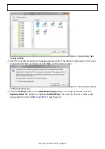
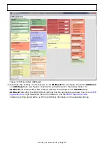
Page 8: ...e used 2 to program the FPGA see Figure 4 Click Yes and the window closes Figure 4 VisualAnalog Default Configuration Message Click the Settings button on the ADC Data Capture block In the pop up wind...

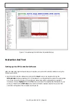
Page 9: ...m right corner of the window see Figure 6 to see what is shown in Figure 7 Change the features and capture settings by consulting the detailed instructions in the AN 905 2 Application Note VisualAnalo...

Page 10: ...tware by going to the Start menu or by double clicking the 1 SPIController software desktop icon If prompted for a configuration file select the appropriate one If not check the title bar of the windo...

Page 11: ...Rev 05 Jun 2013 16 37 Page 11 Figure 8 SPI Controller CHIP ID 1 Box Click the New DUT button in the SPIController window see Figure 9 2...

Page 12: ...divider use the drop down box to select the correct clock divide ratio if necessary The Nyquist Clock is selected by default If using the RF Clock make sure to configure the device in this tab For ad...

Page 13: ...to set up the part in the desired mode The ADCBase0 tab settings affect ADC settings whereas the settings on the ADCBase1 and ADCBase2 tabs affect the JESD204B link settings See the appropriate part d...

Page 14: ...Rev 05 Jun 2013 16 37 Page 14 Figure 11 SPI Controller Example ADCBase1 Page...

Page 15: ...led in Red in VisualAnalog Toolbar Collapsed Display Adjusting the Amplitude of the Input Signal The next step is to adjust the amplitude of the input signal for each channel as follows Adjust the amp...

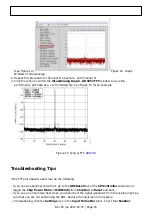
Page 16: ...Typical FFT AD9253 Troubleshooting Tips If the FFT plot appears abnormal do the following If you see an abnormal noise floor go to the ADCBase0 tab of the SPIController window and toggle the Chip Powe...

Page 17: ...curely connected to the HSC ADC EVALDZ board Make sure that the FPGA has been programmed by verifying that the DONE LED is illuminated on the HSC ADC EVALDZ board If this LED is not illuminated make s...

Reviews: