background image

AD7091R User Guide 

UG-409 


Rev. 0 | Page 5 of 20 

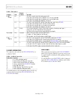
Table 2. Link Options 

Category 

Link 

Default 

Position 

Function 

Buffer 

Settings 

LK1 

This link is used to select the analog signal path. 
In Position A, the analog signal is buffered via U2, a unity gain buffer.  
In Position B, the analog signal is buffered via U3, a unity gain buffer. 
In Position C, the analog signal bypasses U2 and U3. 

LK2 

This link is used to select the source of the analog input signal to the 

AD7091R

In Position A, the analog signal is sourced via the U2 op amp.  
In Position B, the analog signal is sourced via the U3 op amp.  
In Position C, the analog signal bypasses U2 and U3. 

LK3 

Fitted 

This resistor link option is used to select a biased signal as the analog input signal. 
Fitted—bias up circuit connected to the signal path.  
Not fitted—bias up circuit disconnected from the signal path. 

Termination 

LK4 

Inserted 

Adds a 51 Ω termination resistor to AGND at VIN.  
Inserted—51 Ω termination on the VIN input. 
Not inserted—no 51 Ω termination on the VIN input. 

Power 

Supplies 

LK5 

This link is used to select the source of the VDRIVE supply for the 

AD7091R

In Position A, the VDRIVE supply is sourced externally via the J3 connector. 
In Position B, the VDRIVE supply is sourced from the 

EVAL-SDP-CB1Z

 via the J4 connector. 

LK6 

This link is used to select the source of the VDD supply for the 

AD7091R

 and on-board buffers. 

In Position A, the VDD supply is sourced internally from the on-board power supplies. 
In Position B, the VDD supply is sourced externally via the J2 connector. 


SOCKETS/CONNECTORS 

The connectors and sockets on the 

EVAL-AD7091RSDZ

 are as 

outlined in Table 3. 

Table 3. On-Board Connectors  

Connector  Function 

J1 

9 V, 2.0 mm dc jack connector 

J2 

External VDD and AGND power connector 

J3 

External VDRIVE and DGND power connector 

J4 

120-way connector for 

EVAL-SDP-CB1Z

 interface 

J5 

VIN analog input signal 

J6 

VINB analog input signal to bias up circuit 

J7 

External reference voltage connector 

The default interface to this evaluation board is via the 120-way 
connector, which connects the 

EVAL-AD7091RSDZ

 to the 

EVAL-SDP-CB1Z

 board.  


TEST POINTS 

There are numerous test points on the 

EVAL-AD7091RSDZ


board. These test points enable the user to have easy access to 
the signals from the evaluation board for probing, evaluation, 
and debugging. 
It is also possible to access the 

AD7091R

 via the test points to 

operate the 

EVAL-AD7091RSDZ

 in standalone mode without 

the need for the 

EVAL-SDP-CB1Z

 board. 


Summary of Contents for AD7091R

Page 1: ...platform EVAL SDP CB1Z when using evaluation software Signal source EVALUATION BOARD DESCRIPTION The EVAL AD7091RSDZ is a full featured evaluation board designed to allow the user to easily evaluate a...

Page 2: ...ion 4 Hardware Link Options 4 Power Supplies 4 Sockets Connectors 5 Test Points 5 EVAL AD7091RSDZ Basic Hardware Setup 6 Evaluation Board Software 7 Software Installation 7 Launching the Software 8 De...

Page 3: ...ith the enclosed nylon screw nut set to ensure that the boards connect firmly together 5 Connect the power supply adapter included in the kit to Connecter J1 on the EVAL AD7091RSDZ board 6 Connect the...

Page 4: ...See Table 2 for the complete list of link options This evaluation board is supplied with a wall mountable switching power supply that provides a 9 V dc output Connect the supply to a 100 V to 240 V ac...

Page 5: ...RIVE supply is sourced externally via the J3 connector In Position B the VDRIVE supply is sourced from the EVAL SDP CB1Z via the J4 connector LK6 A This link is used to select the source of the VDD su...

Page 6: ...e AD7091R Before connecting power connect the EVAL AD7091RSDZ board to Connector A on the EVAL SDP CB1Z board A nylon screw nut set is included in the EVAL AD7091RSDZ kit and can be used to ensure tha...

Page 7: ...to Step 8 see Figure 7 to Figure 10 to install the EVAL SDP CB1Z drivers Proceed through all of the installation steps allowing the software and drivers to be placed in the appropriate locations Conn...

Page 8: ...e PC The Device Manager can be found by right clicking My Computer Manage Device Manager from the list of System Tools as shown in Figure 11 The EVAL SDP CB1Z SDP B board should appear under ADI Devel...

Page 9: ...nt Panel Picture Prints the software window displayed Save As Picture Saves the front panel as a JPEG file Exit Exits the program Help Menu Open analog com Opens www analog com Control Buttons The EVA...

Page 10: ...FT and Summary The tools shown in Figure 14 allow user control of the different chart displays Figure 14 Chart Tools WAVEFORM CAPTURE Figure 15 illustrates the waveform capture tab The waveform analys...

Page 11: ...in the evaluation software main window and click the SAMPLE button Note that an ac histogram requires a quality signal source applied to the input VIN VINB connectors DC TESTING HISTOGRAM The histogra...

Page 12: ...s to filter the input signal from the ac source There is no sug gested band pass filter but consideration should be taken in the choice Furthermore if using a low frequency band pass filter when the f...

Page 13: ...s such as SNR and THD SAVE FILE The software can save the current captured data for future analysis Go to the File menu and click Save Sample Data The save dialog box opens Save to an appropriate fold...

Page 14: ...15 0 1uF C9 1uF T9 R31 51r C13 4 7nF 2 3 6 OP 4 V 7 V U3 AD8655 C1 1uF C2 0 1uF T2 R10 0r C16 DNI R11 DNI C8 68pF C3 1uF R6 3K R3 DNI R2 3K R5 1K5 C4 0 1uF C5 0 1uF R4 0r C27 DNI R1 1K5 T4 T7 T8 T10 T...

Page 15: ...I N1 7 I N2 5 SD 4 GND 1 OUT1 2 OUT2 6 ERROR 3 NR U6 ADP3303 5 C18 10nF R12 330k C17 10nF C26 1uF J1 3 J1 4 J1 1 J1 2 C19 0 1uF C20 10uF 1 I N 2 GND 3 OUT LC1 EMC_FI LTER 1nF 1 I N 2 GND 3 OUT LC2 EM...

Page 16: ...8 5 SPI _ SEL_ A 8 4 SPI _ MO SI 8 3 SPI _ MI SO 8 2 SPI _ CLK 8 1 GND 8 0 SDA_ 0 7 9 SCL_ 0 7 8 GPI O 1 7 7 GPI O 3 7 6 GPI O 5 7 5 GND 7 4 GPI O 7 7 3 TMR_ B 7 2 TMR_ D 7 1 NC 7 0 NC 6 9 GND 6 8 NC...

Page 17: ...AD7091R User Guide UG 409 Rev 0 Page 17 of 20 Figure 24 EVAL AD7091RSDZTop Side Silkscreen Figure 25 EVAL AD7091RSDZTop Layer Figure 26 EVAL AD7091RSDZBottom Layer 10702 024 10702 025 10702 026...

Page 18: ...r a list of the evaluation boards compatible with the hardware described in this user guide Table 4 Compatible Boards Model1 Description EVAL AD7091RSDZ AD7091R evaluation board EVAL SDP CB1Z Evaluati...

Page 19: ...AD7091R User Guide UG 409 Rev 0 Page 19 of 20 NOTES...

Page 20: ...her party for any reason Upon discontinuation of use of the Evaluation Board or termination of this Agreement Customer agrees to promptly return the Evaluation Board to ADI ADDITIONAL RESTRICTIONS Cus...

Reviews: