background image


Rev 13 Nov 2013 01:51 | Page 13

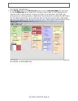
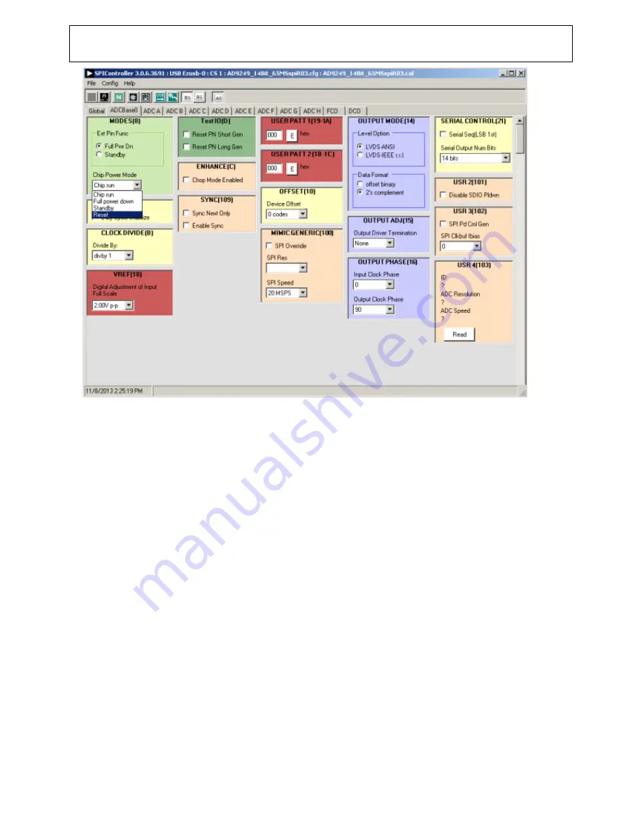
Figure

10. SPI Controller, Chip Power Mode - Digital Reset Selection
Note that other settings can be changed on the ADCBase 0 tab (see Figure 9) and the ADC A

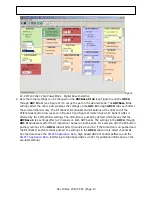
4.

through ADC H tabs (see Figure 11) to set up the part in the desired mode. The ADCBase 0 tab
settings affect the entire part, whereas the settings on the ADC A through ADC H tabs each affect
the selected channel only. The B1 (Bank1), B2 (Bank2) and All buttons at the right end of the
SPIController button row (as seen in Figure 10 and Figure 11) determine which bank of ADCs is
affected by the SPIController settings. The All button is pushed by default which means that the
ADCBase 0 tab settings affect all channels on both ADC banks. The settings in the ADC A through
ADC H will likewise affect their respective channels in both banks. For example, with the All button
pushed, settings in the ADC A tab will affect channels A1 and A2. If the All button is un-pushed and
the B1 (Bank1) button remains pushed, the settings in the ADC A tab will only affect channel A1.
See the data sheet, the 

AN-878 Application Note

High Speed ADC SPI Control Software, and the

AN-877 Application Note

Interfacing to High Speed ADCs via SPI, for additional information on the

available settings.

Summary of Contents for AD9249

Page 1: ...the support circuitry required to operate the ADC in its various modes and configurations The application software used to interface with the device is also described The AD9249 data sheet provides ad...

Page 2: ...on board reference off board reference VisualAnalog and SPIController software interfaces Helpful Documents AD9249 data sheet High speed ADC FIFO evaluation kit HSC ADC EVALDZ HSC ADC EVALDZ Wiki Guid...

Page 3: ...ard as follows Connect the evaluation board to the data capture board as shown in Figure 1 1 On the ADC evaluation board confirm that the jumpers are installed as shown in Figure 2 2 Connect one 6V 2...

Page 4: ...ect the on board LDOs from the power planes Note that in some board configurations some of these might already be uninstalled P102 and P103 headers can be installed to facilitate connection of externa...

Page 5: ...DWN pin can be configured to invoke the STBY standby function instead of power down P1 This jumper sets the ADC for SPI communications with the HSC ADC EVALDZ Connect Pin 1 to Pin 2 for SDIO Pin 4 to...

Page 6: ...owed on the AD9249 65EBZ board Power Connect the switching power supply that is supplied in the evaluation kit between a rated 100V ac to 240V ac 47Hz to 63Hz wall outlet and P101 Analog Input The six...

Page 7: ...ith higher frequency clocks When using the internal divider and a higher input clock frequency remove CR801 to preserve the slew rate of the clock signal The AD9249 65EBZ board is set up to be clocked...

Page 8: ...DUT using the SPI follow the jumper settings for P1 as shown in Table 1 How To Use The Software For Testing Setting up the ADC Data Capture The installers for VisualAnalog and SPIController are in th...

Page 9: ...e 4 VisualAnalog Default Configuration Message To change features to settings other than the default settings click the Expand Display button 3 located on the bottom right corner of the window see Fig...

Page 10: ...to the Start menu or by double clicking the 1 SPIController software desktop icon If prompted for a configuration file select cfg file whose name begins with AD9249 If not prompted check the title ba...

Page 11: ...Rev 13 Nov 2013 01 51 Page 11 Figure 7 SPI Controller CHIP ID 1 Box Click the New DUT button in the SPIController window see Figure 8 2 Figure 8...

Page 12: ...ox to select the correct clock divide ratio if necessary If there is any interruption of the ADC clock during power up or during operation a Digital Reset may be needed to re initialize the ADC Figure...

Page 13: ...determine which bank of ADCs is affected by the SPIController settings The All button is pushed by default which means that the ADCBase 0 tab settings affect all channels on both ADC banks The setting...

Page 14: ...e VisualAnalog toolbar see 6 Figure 12 Figure 12 Run Continuous Run Buttons Encircled in Red in VisualAnalog Toolbar Collapsed Display Adjusting the Amplitude of the Input Signal The next step is to a...

Page 15: ...x00 the ADC is not powered up or SPI communication is not working Check that there is correct power to the AD9249 65EBZ board and to the HSC ADC EVALDZ Check that the USB cable is properly connected f...

Page 16: ...see Figure 12 is clicked do the following Make sure that the evaluation board is securely connected to the HSC ADC EVALDZ board Make sure that the correct FPGA program was installed by clicking the S...

Reviews: