background image


Rev 13 May 2013 17:57 | Page 9

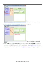
located on the bottom right corner of the window (see Figure 5), to see what is shown in Figure 6.
Change the features and capture settings by consulting the detailed instructions in the 

AN-905

4.

Application Note

VisualAnalog Converter Evaluation Tool Version 1.0 User Manual. After the

changes are made to the capture settings, click the Collapse Display button.

Figure 5. VisualAnalog Window Toolbar, Collapsed Display

Figure 6. VisualAnalog, Main Window Expanded Display

Evaluation And Test

Setting up the SPI Controller Software

After the ADC data capture board setup is complete, set up the SPI controller software using the
following procedure:

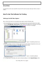
Open the SPI controller software by going to the Start menu or by double-clicking the

1.

SPIController software desktop icon. If prompted for a configuration file, select the appropriate
one. If not, check the title bar of the window to determine which configuration is loaded. If
necessary, choose Cfg Open from the File menu and select the appropriate file based on your
part type. Note that the CHIP ID(1) box should be filled to indicate whether the correct SPI
controller configuration file is loaded (see Figure 7).

Summary of Contents for AD9253

Page 1: ...perate these parts in their various modes and configurations The application software used to interface with the devices is also described The AD9653 AD9253 and AD9633 data sheets provide additional i...

Page 2: ...878 Application Note High Speed ADC SPI Control Software AN 877 Application Note Interfacing to High Speed ADCs via SPI AN 835 Application Note Understanding ADC Testing and Evaluation Design and Inte...

Page 3: ...1 shows the typical bench characterization setup used to evaluate AC performance It is critical that the signal sources used for the analog input and clock have very low phase noise 1 ps rms jitter to...

Page 4: ...e desired frequency and amplitude see the Specifications section in the data sheet of the respective part When connecting the analog input source use of a multipole narrow band band pass filter with 5...

Page 5: ...ate reference voltages from 1 0 V to 1 3 V the AD9253 and AD9633 reference voltage is specified to be 1 0 V J204 Use this jumper to power down the ADC Using the SPI the PDWN pin can be configured to b...

Page 6: ...ovided by the ADR130 This external reference can be connected to the ADC by connecting Pin 4 to Pin 6 on Header J202 Alternatively if an external off board reference is desired connect Pin 2 to Pin1 o...

Page 7: ...J802 labeled CLK PDWN To enable the power down feature add a shorting jumper across J204 at Pin 1 and Pin 2 to connect the PDWN pin to DRVDD Modes of Operation Standalone PIN Mode The AD9653 AD9253 AD...

Page 8: ...pe should be listed in the status 1 bar of the VisualAnalog New Canvas window Select the template that corresponds to the type of testing to be performed see Figure 3 where the AD9253 is shown as an e...

Page 9: ...lay Evaluation And Test Setting up the SPI Controller Software After the ADC data capture board setup is complete set up the SPI controller software using the following procedure Open the SPI controll...

Page 10: ...In the ADCBase 0 tab of the SPIController window find the CLOCK DIVIDE B box see Figure 3 9 If using the clock divider use the drop down box to select the correct clock divide ratio if necessary For...

Page 11: ...he selected channel only See the appropriate part data sheet the AN 878 Application Note High Speed ADC SPI Control Software and the AN 877 Application Note Interfacing to High Speed ADCs via SPI for...

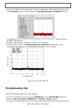
Page 12: ...el D 2 Click the disk icon within the VisualAnalog Graph AD9253 FFT window to save the 3 performance plot data as a csv formatted file See Figure 13 for an example Figure 13 Typical FFT AD9253 Trouble...

Page 13: ...do the following Make sure that the evaluation board is securely connected to the HSC ADC EVALCZ board Make sure that the FPGA has been programmed by verifying that the DONE LED is illuminated on the...

Reviews: