Rev 13 Nov 2013 00:23 | Page 5
accept ~2.8V p-p or 13 dBm sine wave input for the clock. If an external off-board clock source is
used, remove the jumper on P601, and C1109, to disable and disconnect the on-board crystal
oscillator.
Output Signals
The default setup uses the Analog Devices high speed converter evaluation platform (
) for data capture. The serial LVDS outputs from the ADC are routed to Connector
P1302 using 100Ω differential traces. For more information on the data capture board and its optional
settings, visit
Jumper Settings
Set the jumper settings/link options on the evaluation board for the required operating modes before
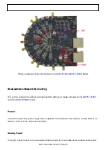
powering on the board. The functions of the jumpers are described in Table 1. Figure 2 shows the
default jumper settings.
Table 1. Jumper Settings
Jumper
Description
J203
Use this jumper to power down the ADC. Using the SPI, the PDWN pin can be configured
to be STBY (standby).
J1001 and
J1002
These jumpers enable the optional ADL5565 amplifiers on Channels G and H,
respectively. Connect pin 2 to pin 3 for default (amplifier disabled) operation.
J301
This jumper sets the ADC for SPI communications with the
Connect Pin 1 to Pin 2 for SDIO, Pin 4 to Pin 5 for SCLK, and Pin 8 to Pin 9 for CSB.
J1103
This jumper enables the on-board crystal oscillator. Remove this jumper if an external
off-board clock source is used.
J202
This jumper selects between internal V
REF
and external V
REF
.
To choose the internal 1V reference, connect Pin 3 (DUT_SENSE) to Pin 5 (GND).
To use the on-board
1V reference, connect Pin 2 (DUT_SENSE) to Pin 1 (AVDD),
and connect Pin 4 (DUT_VREF) to Pin 6 (EXT_REF).
To apply a reference voltage from an external off-board source, connect Pin 2
(DUT_SENSE) to Pin 1 (AVDD) and apply the reference voltage to Pin 4 (DUT_VREF). The
AD9257 and AD9637 reference voltage is specified to be 1.0 V.
P1201
Header to observe AD9517 (optional clock generator) Digital Lock Detect pins.

