Rev 13 Nov 2013 00:23 | Page 8
SDIO/DFS (J301 Pin 2) Voltage
Device Mode
1.8V_DUT_AVDD (jumper J301 Pin 2 to Pin 3) Twos Complement
GND (“float” J301 Pin 2)
Offset Binary
Table 3. Digital Test Pattern Pin Settings
SCLK/DTP (J301 Pin 5) Voltage
Output Format
GND (“float” J301 Pin 5)
Normal Operation
1.8V_DUT_AVDD (jumper J301 Pin 5 to Pin 6) 10 0000 0000 0000
Note that the above settings only apply when CSB is tied high (J301 Pin 8 “floating”) at power up.
Additional information on the Standalone (PIN) Mode is provided in the
and
sheets.
Default Mode
To operate the device under test (DUT) using the SPI, follow the jumper settings for J301 as shown in
Table 1.
How To Use The Software For Testing
Setting up the ADC Data Capture
After configuring the board, set up the ADC data capture using the following steps:
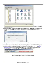
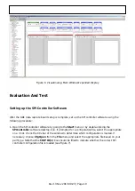
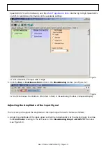
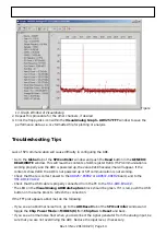
Open VisualAnalog on the connected PC. The appropriate part type should be listed in the status
1.
bar of the VisualAnalog – New Canvas window. Select the template that corresponds to the type
of testing to be performed (see Figure 3, where the

