background image


Rev 03 Jun 2015 18:39 | Page 15

the VisualAnalog Input Formatter matches the data format selected in the SPIController
ADCBase0 OUTPUT MODE(14)
 window.
For proper capture, DCO-to-data output timing might need to be adjusted. In the ADCBase0 tab of

SPIController (shown in Figure 9), in the OUTPUT DELAY(17) field, check the DCO DELAY EN box, and
try various output delay settings to see if capture improves.

If the FFT appears normal but the performance is poor, check the following:

That an appropriate filter is used on the analog input.

That the signal generators for the clock and the analog input are clean (low phase noise).

That if noncoherent sampling is being used, change the analog input frequency slightly.

That the SPI configuration file matches the product being evaluated.

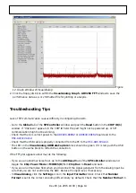
If the FFT window remains blank after Run in VisualAnalog (see Figure 12) is clicked, do the following:

Make sure that the evaluation board is securely connected to the 

HSC-ADC-EVALCZ

 board.

Make sure that the FPGA has been programmed by verifying that the DONE LED is illuminated on

the 

HSC-ADC-EVALCZ

 board. If this LED is not illuminated, make sure that the U4 switch on the

board is in the correct position for USB CONFIG.
Make sure that the correct FPGA program was installed by clicking the Settings icon in the ADC

Data Capture block in VisualAnalog. Then, select the FPGA tab and verify that the proper FPGA bin
file is selected for the device.

© Analog Devices, Inc. All rights reserved. Trademarks and
registered trademarks are the property of their respective owners.

www.analog.com

Summary of Contents for AD9266

Page 1: ...ication software used to interface with the devices is also described The AD9266 AD9649 AD9629 and AD9609 data sheets provide additional information and should be consulted when using the evaluation b...

Page 2: ...Evaluation Tool Version 1 0 User Manual AN 878 Application Note High Speed ADC SPI Control Software AN 877 Application Note Interfacing to High Speed ADCs via SPI AN 835 Application Note Understanding...

Page 3: ...of the HSC ADC EVALCZ is in the 2 5V position On the ADC evaluation board confirm that the jumpers are installed as shown in Figure 2 The 5 configuration in Figure 2 enables SPI control of the device...

Page 4: ...ds might already be uninstalled P102 and P103 need to be installed to connect external bench supplies to the board and E109 E110 E111 E112 and E113 need to be populated to connect P102 and P103 to the...

Page 5: ...ls power down and standby modes In the case where MODE_OR is configured as an input connecting Pin 2 to Pin 3 invokes the programmed pin function see the product datasheet for more information J302 J3...

Page 6: ...llowed on the AD9266 80EBZ and the AD9649 80EBZ boards Power Connect the switching power supply that is supplied in the evaluation kit between a rated 100 V ac to 240 V ac 47 Hz to 63 Hz wall outlet a...

Page 7: ...k frequency remove CR601 to preserve the slew rate of the clock signal The AD9266 80EBZ AD9649 80EBZ AD9629 80EBZ and AD9609 80EBZ boards are set up to be clocked through the transformer coupled input...

Page 8: ...information on the standalone pin mode is provided in the AD9266 AD9649 AD9629 and AD9609 data sheets Default Mode To operate the device under test DUT using the SPI follow the jumper settings for J30...

Page 9: ...mmed If VisualAnalog does not prompt for programming the FPGA select the ADC Data Capture Settings window and click on the Capture Board tab In the FPGA box select program to configure the FPGA Figure...

Page 10: ...ng the following procedure Open the SPI controller software by going to the Start menu or by double clicking the 1 SPIController software desktop icon If prompted for a configuration file select the a...

Page 11: ...Rev 03 Jun 2015 18 39 Page 11 controller configuration file is loaded see Figure 7 Figure 7 SPI Controller CHIP ID 1 Box Click the New DUT button in the SPIController window see Figure 8 2...

Page 12: ...own menu to select the correct clock divide ratio as desired If there is any interruption of the ADC clock during power up or during operation a digital reset may be needed to reinitialize the ADC Fig...

Page 13: ...peed ADCs via SPI for additional information on the available settings Click the Run or Continuous Run button in the VisualAnalog toolbar see Figure 11 5 Figure 11 Run Continuous Run Buttons Encircled...

Page 14: ...he HSC ADC EVALCZ Check that the USB cable is properly connected from the PC to the HSC ADC EVALCZ The LED on the VisualAnalog ADCDataCapture block should be green If it is red push the USB button on...

Page 15: ...g input frequency slightly That the SPI configuration file matches the product being evaluated If the FFT window remains blank after Run in VisualAnalog see Figure 12 is clicked do the following Make...

Reviews: