background image


Rev 13 Nov 2013 01:53 | Page 3

Design and Integration Files

Schematics, layout files, bill of materials

 <Coming Soon>

Equipment Needed

Analog signal source(s) and antialiasing filter(s)

Sample clock source (if not using the on-board crystal oscillator)

Switching power supply (6.0V, 2.5A) for AD9681-125EBZ

Switching power supply (12V, 3,3A) for HSC-ADC-EVALDZ

PC running Windows®

USB 2.0 port

AD9681-125EBZ

 board

HSC-ADC-EVALDZ

 FPGA-based data capture kit

Getting Started

This section provides quick start procedures for using the 

AD9681-125EBZ

 board. Both the default

and optional ADC settings are described.

Configuring the Board

Before using the software for testing, configure the evaluation board as follows:

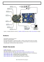
Connect the evaluation board to the data capture board, as shown in Figure 1.

1.

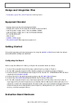
On the ADC evaluation board, confirm that the jumpers are installed as shown in Figure 2.

2.

Connect one 6V, 2.5A switching power supply (such as the CUI, Inc., EPS060250UH-PHP-SZ that is

3.

supplied) to the 

AD9681-125EBZ

.

Connect the 12V, 3.3A switching power supply to the 

HSC-ADC-EVALDZ

 board.

4.

Connect the 

HSC-ADC-EVALDZ

 board (P702) to the PC using a USB cable.

5.

On the ADC evaluation board, use a clean signal generator with low phase noise to provide an

6.

input signal to the desired channel(s). Use a shielded, RG-58, 50Ω coaxial cable (optimally 1 m or
shorter) to connect the signal generator. For best results, use a narrow-band, band-pass filter with
50Ω terminations and an appropriate center frequency. (Analog Devices, Inc. uses TTE, Allen
Avionics, and K&L band-pass filters.)

Evaluation Board Hardware


Summary of Contents for AD9681

Page 1: ...the support circuitry required to operate the ADC in its various modes and configurations The application software used to interface with the device is also described The AD9681 data sheet provides a...

Page 2: ...on board reference off board reference VisualAnalog and SPIController software interfaces Helpful Documents AD9681 data sheet High speed ADC FIFO evaluation kit HSC ADC EVALDZ HSC ADC EVALDZ Wiki Guid...

Page 3: ...oard as follows Connect the evaluation board to the data capture board as shown in Figure 1 1 On the ADC evaluation board confirm that the jumpers are installed as shown in Figure 2 2 Connect one 6V 2...

Page 4: ...ect the on board LDOs from the power planes Note that in some board configurations some of these might already be uninstalled P102 and P103 headers can be installed to facilitate connection of externa...

Page 5: ...DWN pin can be configured to invoke the STBY standby function instead of power down P1 This jumper sets the ADC for SPI communications with the HSC ADC EVALDZ Connect Pin 1 to Pin 2 for SDIO Pin 4 to...

Page 6: ...ed on the AD9681 125EBZ board Power Connect the switching power supply that is supplied in the evaluation kit between a rated 100V ac to 240V ac 47Hz to 63Hz wall outlet and P101 Analog Input The eigh...

Page 7: ...h higher frequency clocks When using the internal divider and a higher input clock frequency remove CR801 to preserve the slew rate of the clock signal The AD9681 125EBZ board is set up to be clocked...

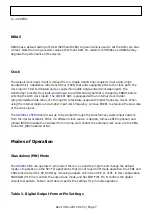
Page 8: ...e the device under test DUT using the SPI follow the jumper settings for P1 as shown in Table 1 How To Use The Software For Testing Setting up the ADC Data Capture The installers for VisualAnalog and...

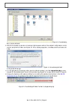
Page 9: ...e 4 VisualAnalog Default Configuration Message To change features to settings other than the default settings click the Expand Display button 3 located on the bottom right corner of the window see Fig...

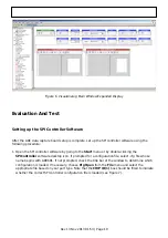
Page 10: ...to the Start menu or by double clicking the 1 SPIController software desktop icon If prompted for a configuration file select cfg file whose name begins with AD9681 If not prompted check the title ba...

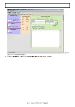
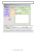
Page 11: ...Rev 13 Nov 2013 01 53 Page 11 Figure 7 SPI Controller CHIP ID 1 Box Click the New DUT button in the SPIController window see Figure 8 2...

Page 12: ...ivider use the drop down box to select the correct clock divide ratio if necessary If there is any interruption of the ADC clock during power up or during operation a Digital Reset may be needed to re...

Page 13: ...Rev 13 Nov 2013 01 53 Page 13 Figure 9 SPI Controller CLOCK DIVIDE B Box Figure...

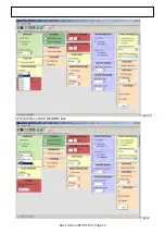
Page 14: ...settings affect all channels on both ADC banks The settings in the ADC A through ADC D will likewise affect their respective channels in both banks For example with the All button pushed settings in...

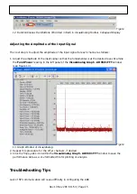
Page 15: ...so that the fundamental is at the desired level Examine 1 the Fund Power reading in the left panel of the VisualAnalog Graph AD9681 FFT window see Figure 13 Figure 13 Graph Window of VisualAnalog Repe...

Page 16: ...ter matches the data format selected in the SPIController ADCBase0 OUTPUT MODE 14 window Repeat for the other channels If the FFT appears normal but the performance is poor check the following Make su...

Reviews: