Rev 13 Nov 2013 01:53 | Page 8
SDIO/OLM (P1 Pin 2) Voltage
Device Mode
1.8V_DUT_AVDD (jumper P1 Pin 2 to Pin 3) Two-lane. 1× frame, 16-bit serial output
GND (“float” P1 Pin 2)
One-lane. 1× frame, 16-bit serial output
Table 3. Digital Test Pattern Pin Settings
SCLK/DTP (P1 Pin 5) Voltage
Output Format
GND (“float” P1 Pin 5)
Normal Operation
1.8V_DUT_AVDD (jumper P1 Pin 5 to Pin 6) 10 0000 0000 0000
Note that the above settings only apply when CSB1 and CSB2 are tied high (P1 Pin 8 and Pin 11
“floating”) at power up.
Additional information on the Standalone (PIN) Mode is provided in the
data sheet.
Default Mode
To operate the device under test (DUT) using the SPI, follow the jumper settings for P1 as shown in
Table 1.
How To Use The Software For Testing
Setting up the ADC Data Capture
The installers for VisualAnalog and SPIController are in the following locations:
ftp://ftp.analog.com/pub/HSSP_SW/VisualAnalog/VisualAnalog_Setup.exe
ftp://ftp.analog.com/pub/adispi/A2DComponents/Install/SPIController_Setup.exe
Run these installers on the PC that is connected to the evaluation setup before proceeding.
After configuring the board hardware, set up the ADC data capture using the following steps:
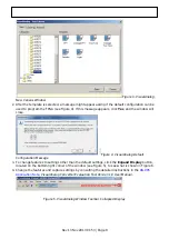
Start VisualAnalog on the connected PC. The appropriate part type should be listed in the status
1.
bar of the VisualAnalog – New Canvas window. Select the template that corresponds to the type
of testing to be performed (see Figure 3).


