AD9776A/AD9778A/AD9779A
Rev. B | Page 32 of 56
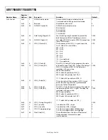
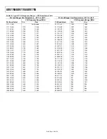
Register
Address
Bits
Register Name
Parameter
Function
Default
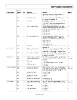
AUX DAC2 Control
0x12
0x11
1:0
7:0
Auxiliary DAC2 Data[9:8]
Auxiliary DAC2 Data[7:0]
Auxiliary DAC2 Data[9:0] is the 10-bit output
current control word. Magnitude of the auxiliary
DAC current increases with increasing value. Bit 9 is
the MSB and Bit 0 is the LSB.
00
00000000
0x12
7
Auxiliary DAC2 sign
0: AUX2_P active.
1: AUX2_N active.
0
0x12 6 Auxiliary DAC2 current
direction
0: source.
1: sink.
0
0x12
5
Auxiliary DAC2 power-down
0: auxiliary DAC2 on.
1: auxiliary DAC2 off.
0
0x13 to
0x18
Reserved
Interrupt
0x19
7
Data timing error IRQ
Read only. Active high indicates a timing violation
occurred on the input data port. The IRQ is latched.
This bit is cleared when the Interrupt register is read.
0
0x19
6
Sync timing error IRQ
Read only. Active high indicates a timing violation
occurred on the SYNC_I input. The IRQ is latched.
This bit is cleared when the Interrupt register is read.
0
0x19
4
Data timing error type
Read only. Indicates the timing error type.
0: hold time violation.
1: setup time violation.
Meaningful when data timing error IRQ is active.
0
0x19
3
Data timing error IRQ enable
0: data timing error IRQ is masked.
1: data timing error IRQ is enabled.
0
0x19
2
Sync timing error IRQ enable
0: sync timing error IRQ is masked.
1: sync timing error IRQ is enabled.
0
0x19 0 Internal
sync
loopback
The received SYNC_O signal is looped back to the
SYNC_I signal.
0
Version
0x1F
7:0
Version[7:0]
Indicates device hardware revision number.
00000111

