AD9776A/AD9778A/AD9779A
Rev. B | Page 45 of 56
RBIP
50
Ω
RBIN
50
Ω
93
90
92
21
22
IBBN
IBBP
AD9779A
RBQN
50
Ω
RBQP
50
Ω
84
87
89
83
86
9
10
RSLI
100
Ω
RSLQ
100
Ω
OUT1_N
AUX1_N
AUX2_N
OUT1_P
AUX1_P
OUT2_P
AUX2_P
OUT2_N
QBBP
QBBN
LPI
390nH
LNI
390nH
82pF
C1I
39pF
C2I
LNQ
390nH
LPQ
390nH
82pF
C3Q
39pF
C2Q
250
Ω
500
Ω
500
Ω
500
Ω
500
Ω
250
Ω
250
Ω
250
Ω
82pF
C3I
82pF
C1Q
06
452
-09
3
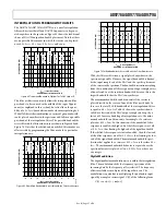
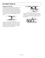
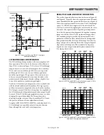
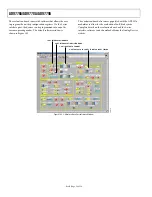
Figure 79. Typical Use of Auxiliary DACs AC Coupling to
Quadrature Modulator
LO FEEDTHROUGH COMPENSATION
The LO feedthrough compensation is the most complex of all
three operations. This is due to the structure of the offset aux-
iliary DACs, as shown in Figure 78. To achieve LO feedthrough
compensation in a circuit, each of four outputs of these auxiliary
DACs can be connected through a 500 Ω resistor to ground
and through a 250 Ω resistor to one of the four quadrature
modulator signal inputs. The purpose of these connections is
to drive a very small amount of current into the nodes at the
quadrature modulator inputs, therefore adding a slight dc bias
to one of the quadrature modulator signal inputs.
To achieve LO feedthrough compensation, the user should start
with the default conditions of the auxiliary DAC sign registers,
and then increment the magnitude of one or the other auxiliary
DAC output currents. While this is being done, the amplitude of
the LO feedthrough at the quadrature modulator output should
be sensed. If the LO feedthrough amplitude increases, try either
changing the sign of the auxiliary DAC being adjusted or
adjusting the output current of the other auxiliary DAC. It may
take practice before an effective algorithm is achieved.
Using the AD9776A/AD9778A/AD9779A evaluation board, the
LO feedthrough can typically be adjusted down to the noise
floor, although this is not stable over temperature.
RESULTS OF GAIN AND OFFSET CORRECTION
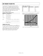
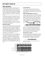
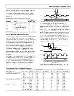
The results of gain and offset correction can be seen in Figure 80
and Figure 81. Figure 80 shows the output spectrum of the quad-
rature demodulator before gain and offset correction. Figure 81
shows the output spectrum after correction. The LO feedthrough
spur at 2.1 GHz has been suppressed to the noise level. This
result can be achieved by applying the correction, but the correc-
tion needs to be repeated after a large change in temperature.
Note that the gain matching improved the negative frequency
image rejection, but there is still a significant image present.
The remaining image is now due to phase mismatch in the
quadrature modulator. Phase mismatch can be distinguished
from gain mismatch by the shape of the image. Note that the
image in Figure 80 is relatively flat and the image in Figure 81
slopes down with frequency. Phase mismatch is frequency
dependent, so an image dominated by phase mismatch has
this sloping characteristic.
06
45
2-
3
04
SPAN 200MHz
CENTER 2.1GHz
REF LVL
0dBm
20MHz
0
–100
–10
–20
–30
–40
–50
–60
–70
–80
–90
RBW
3kHz
REF ATT
30dB
VBW
3kHz
MIXER
–40dBm
SWT
56s
UNIT
dBm
Figure 80. AD9779A and ADL5372 with a Multitone Signal at 2.1 GHz,
No Gain or LO Compensation
06
45
2-
30
5
SPAN 200MHz
CENTER 2.1GHz
REF LVL
0dBm
20MHz
0
–100
–10
–20
–30
–40
–50
–60
–70
–80
–90
RBW
20kHz
REF ATT
20dB
VBW
20kHz
MIXER
–40dBm
SWT
1.25s
UNIT
dBm
Figure 81. AD9779A and ADL5372 with a Multitone Signal at 2.1 GHz,
Gain and LO Compensation Optimized

