background image

AD9776A/AD9778A/AD9779A 


Rev. B | Page 46 of 56 

INPUT DATA PORTS 

DUAL PORT MODE 

The AD9776A/AD9778A/AD9779A can operate in two data 
input modes: dual port mode and single port mode. For the 
default dual port mode (single port bit = 0), each DAC receives 
data from a dedicated input port. In single port mode (single 
port bit = 1), both DACs receive data from Port 1. In single port 
mode, DAC1 and DAC2 data is interleaved, and the TXENABLE 
input is used to steer data to the intended DAC. In dual port 
mode, the TXENABLE input is used to power down the digital 
data path. 

In dual port mode, data for each DAC is received on the 
respective input bus (P1D[15:0] or P2D[15:0]). I and Q data 
arrive simultaneously and are sampled on the rising edge of the 
DATACLK signal. The TXENABLE signal must be high to enable 
the transmit path. 

INPUT DATA REFERENCED TO DATACLK 

The simplest method of interfacing to the AD9776A/AD9778A/ 
AD9779A is when the input data is referenced to the DATACLK 
output. The DATACLK output is a buffered version (with some 
fixed delay) of the internal clock that is used to latch the input 
data. Therefore, if setup and hold times of the input data with 
respect to DATACLK are met, the input data is latched correctly. 
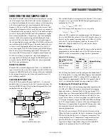
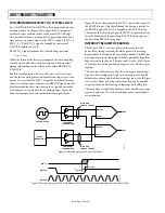
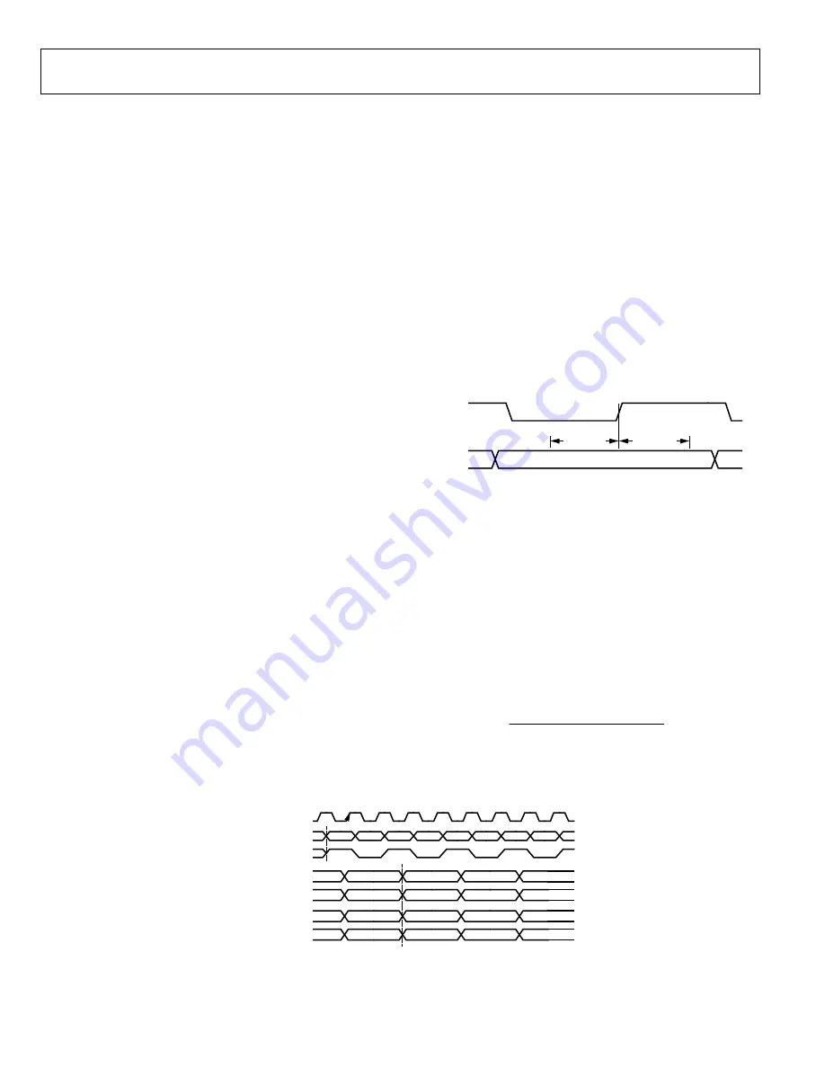
Detailed timing diagrams for the single and dual port cases 
using DATACLK as the timing reference are shown in Figure 82

In dual port mode, the data must be delivered at the input data 
rate. In single port mode, data must be delivered at twice the 
input data rate of each DAC. Because the data inputs function 
up to a maximum of 300 MSPS, it is practical to operate with 
input data rates up to 150 MHz per DAC in single port mode. 

In dual port and single port modes, a data clock output 
(DATACLK) signal is available as a fixed time base with which 
to drive data from an FPGA or other data source. This output 
signal operates at the input data rate.  

DATACLK

DATA

t

SDATACLK

t

HDATACLK

064

52

-30

8


SINGLE PORT MODE 

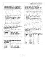
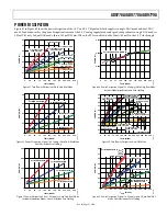
In single port mode, data for both DACs is received on the Port 1 
input bus (P1D[15:0]). I and Q data samples are interleaved and 
are sampled on the rising edges of DATACLK. Along with the 
data, a framing signal must be supplied on the TXENABLE 
input (Pin 39), which steers incoming data to its respective DAC. 
When TXENABLE is high, the corresponding data-word is sent 
to the I DAC. When TXENABLE is low, the corresponding data is 
sent to the Q DAC. The timing of the digital interface in 
interleaved mode is shown in Figure 83

Figure 82. Input Data Port Timing, Data Referenced to DATACLK 

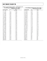
Table 28 shows the setup and hold time requirements for the 
input data over the operating temperature range of the device. 
Also shown is the keep out window (KOW). The keep out 
window is the sum of the setup and hold times of the interface. 
This is the minimum amount of time valid data must be 
presented to the device to ensure proper sampling. 

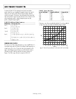
DATACLK Frequency Settings 

The DATACLK signal is derived from the internal DAC sample 
clock, DACCLK. The frequency of the DATACLK output depends 
on several programmable settings. Normally, the frequency of 
DATACLK is equal to the input data rate. The relationship 
between the frequency of DACCLK and DATACLK is 

The Q first bit (Register 0x02, Bit 0) controls the pairing order 
of the input data. With the Q first bit set to the default of 0, the 
I-Q pairing sent to the DACs is the two input data-words 
corresponding to TXENABLE low followed by TXENABLE 
high. With the Q first bit set to 1, the I-Q pairing sent to the 
DACs is the two input data-words corresponding to TXENABLE 
high, followed by TXENABLE low. Note that with either order 
pairing, the data sent with TXENABLE high is directed to the 
I DAC, and the data sent with TXENABLE low is directed to the 
Q DAC. 

DATACLKDIV

SP

ZS

IF

f

f

DACCLK

DATACLK

×

×

×

=


where the variables 

IF

ZS

SP

, and 

DATACLKDIV

 have the 

values shown in Table 27


06

45

2-

30

6

DATACLK

P1D[15:0]

TXENABLE

I DAC[15:0]

Q DAC[15:0]

I DAC[15:0]

Q DAC[15:0]

Q FIRST = 1

Q FIRST = 0

P1D1

P1D2

P1D3

P1D4

P1D5

P1D6

P1D7

P1D8

P1D1

P1D3

P1D5

P1D1

P1D0

P1D3

P1D5

P1D2

P1D4

P1D6

P1D2

P1D4


Figure 83. Single Port Mode Digital Interface Timing 


Summary of Contents for AD9776A

Page 1: ...TION The AD9776A AD9778A AD9779A are dual 12 14 16 bit high dynamic range digital to analog converters DACs that provide a sample rate of 1 GSPS permitting a multicarrier generation up to the Nyquist...

Page 2: ...SB Transfers 27 3 Wire Interface Register Map 28 Interpolation Filter Architecture 33 Interpolation Filter Bandwidth Limits 37 Inverse Sinc Filter 38 Sourcing the DAC Sample Clock 39 Direct Clocking 3...

Page 3: ...alibration with Memory Section 41 Changes to Set and Forget Device Option Section 41 Added Table 26 41 Changes to Internal Reference Section 43 Changed Transmit Path Gain and Offset Correction Heading...

Page 4: ...DAC REFCLK REFCLK OUT1_P OUT1_N AUX1_P AUX1_N AUX2_P AUX2_N OUT2_P OUT2_N GAIN GAIN GAIN GAIN 16 BIT Q DAC 2 SINC 1 I LATCH DELAY LINE Q LATCH P2D 15 0 P1D 15 0 SYNC_O SYNC_I DATACLK 2 2 2 n fDAC 8 n...

Page 5: ...998 1 998 1 998 1 998 1 998 1 998 mA Output Compliance Range Source 0 1 6 0 1 6 0 1 6 V Output Compliance Range Sink 0 8 1 6 0 8 1 6 0 8 1 6 V Output Resistance 1 1 1 M Auxiliary DAC Monotonicity Guar...

Page 6: ...IDTH 100 100 mV Input Differential Hysteresis VIDTHH VIDTHL 20 mV Receiver Differential Input Impedance RIN 80 120 LVDS Input Rate Additional limits on fSYNC_I apply see description of Register 0x05 B...

Page 7: ...modulation 297 DACCLK cycles Inverse Sync 18 DACCLK cycles 3 WIRE INTERFACE Maximum Clock Rate SCLK 40 MHz Minimum Pulse Width High tPWH 12 5 ns Minimum Pulse Width Low tPWL 12 5 ns Setup Time tDS SD...

Page 8: ...LATION DISTORTION IMD fDAC 200 MSPS fOUT 50 MHz 87 87 91 dBc fDAC 400 MSPS fOUT 60 MHz 80 85 85 dBc fDAC 400 MSPS fOUT 80 MHz 75 81 81 dBc fDAC 800 MSPS fOUT 100 MHz 75 80 81 dBc NOISE SPECTRAL DENSIT...

Page 9: ...3 V to 0 3 V I120 VREF IPTAT AGND 0 3 V to AVDD33 0 3 V OUT1_P OUT1_N OUT2_P OUT2_N AUX1_P AUX1_N AUX2_P AUX2_N AGND 1 0 V to AVDD33 0 3 V P1D 15 0 P2D 15 0 DGND 0 3 V to DVDD33 0 3 V DATACLK TXENABL...

Page 10: ...DOMAIN NC NO CONNECT 06452 002 NOTES 1 FOR OPTIMAL THERMAL PERFORMANCE THE EXPOSED PAD SHOULD BE SOLDERED TO THE GROUND PLANE FOR THE 100 LEAD THERMALLY ENHANCED TQFP PACKAGE Figure 3 AD9776A Pin Conf...

Page 11: ...SDIO 3 Wire Interface Port Data Input Output 68 SCLK 3 Wire Interface Port Clock Pin No Mnemonic Description 69 CSB 3 Wire Interface Port Chip Select Bar 70 RESET Reset Active High 71 IRQ Interrupt R...

Page 12: ...THE EXPOSED PAD SHOULD BE SOLDERED TO THE GROUND PLANE FOR THE 100 LEAD THERMALLY ENHANCED TQFP PACKAGE Figure 4 AD9778A Pin Configuration Table 8 AD9778A Pin Function Descriptions Pin No Mnemonic Des...

Page 13: ...Data Input Output 68 SCLK 3 Wire Interface Port Clock 69 CSB 3 Wire Interface Port Chip Select Bar 70 RESET Reset Active High Pin No Mnemonic Description 71 IRQ Interrupt Request 72 AGND Analog Groun...

Page 14: ...SHOULD BE SOLDERED TO THE GROUND PLANE FOR THE 100 LEAD THERMALLY ENHANCED TQFP PACKAGE Figure 5 AD9779A Pin Configuration Table 9 AD9779A Pin Function Descriptions Pin No Mnemonic Description Pin No...

Page 15: ...Interface Port Data Input Output 68 SCLK 3 Wire Interface Port Clock 69 CSB 3 Wire Interface Port Chip Select Bar 70 RESET Reset Active High Pin No Mnemonic Description 71 IRQ Interrupt Request 72 AGN...

Page 16: ...ATA 200MSPS fDATA 250MSPS 06452 007 Figure 8 AD9779A In Band SFDR vs fOUT 1 Interpolation 100 50 0 100 fOUT MHz SFDR dBc 90 80 70 60 20 40 60 80 fDATA 160MSPS fDATA 200MSPS fDATA 250MSPS 06452 008 Fig...

Page 17: ...fOUT MHz SFDR dBc 90 80 70 60 10 20 30 40 fDATA 50MSPS fDATA 100MSPS fDATA 125MSPS 06452 013 Figure 14 AD9779A Out of Band SFDR vs fOUT 8 Interpolation 100 50 0 40 fOUT MHz SFDR dBc 90 80 70 60 10 20...

Page 18: ...TA 200MSPS fDATA 100MSPS 06452 019 Figure 20 AD9779A Third Order IMD vs fOUT 4 Interpolation fOUT MHz IMD dBc fDATA 75MSPS fDATA 125MSPS fDATA 100MSPS 90 100 80 70 60 50 450 425 400 375 350 325 300 27...

Page 19: ...TEN 20dB EXT REF DC COUPLED 06452 023 Figure 26 AD9779A Single Tone 4 Interpolation fDATA 100 MSPS fOUT 30 MHz STOP 400 0MHz SWEEP 1 203s 601 pts VBW 20kHz START 1 0MHz RES BW 20kHz REF 0dBm PEAK Log...

Page 20: ...22 88 MSPS fDAC 4 Modulation 55 90 85 80 75 70 65 60 0 260 240 220 200 180 160 140 120 100 80 60 40 20 fOUT MHz ACLR dBc 06452 301 3dBFS PLL DISABLED 6dBFS PLL DISABLED 0dBFS PLL ENABLED 0dBFS PLL DIS...

Page 21: ...52 036 Figure 39 AD9778A In Band SFDR vs fOUT 2 Interpolation 90 0 250 fOUT MHz ACLR dBc 70 80 60 25 50 75 100 125 150 175 200 225 FIRST ADJACENT CHANNEL SECOND ADJACENT CHANNEL THIRD ADJACENT CHANNEL...

Page 22: ...at 6 dBFS fDATA 200 MSPS 0 4 0 4096 CODE INL 12 BIT LSB 0 4 512 1024 2560 2048 1536 3072 3584 0 3 0 2 0 1 0 0 1 0 2 0 3 06452 041 Figure 44 AD9776A Typical INL 0 20 0 4096 CODE DNL 12 BIT LSB 2048 0...

Page 23: ...0 78 05 77 73 dBm 87 67 90 73 90 41 LOWER dBc 75 30 77 99 77 50 dBm 87 97 90 66 90 17 UPPER REF 25 29dBm AVG log 10dB PAVG 10 W1 S2 ATTEN 4dB 06452 046 Figure 49 AD9776A Single Carrier W CDMA 4 Interp...

Page 24: ...tart of the output transition In Band Spurious Free Dynamic Range SFDR In band SFDR is the difference in decibels between the peak amplitude of the output signal and the peak spurious signal between d...

Page 25: ...D9776A AD9778A AD9779A PLL are wider than those for the AD9776 AD9778 AD9779 This means that the AD9776A AD9778A AD9779A PLL remains in lock in a given range over a wider temperature range than the AD...

Page 26: ...ransfer is a read or write the number of bytes in the data transfer and the starting register address for the first byte of the data transfer The first eight SCLK rising edges of each communication cy...

Page 27: ...SB Multibyte data transfers in MSB first format start with an instruction byte that includes the register address of the most significant data byte Subsequent data bytes should follow from high addres...

Page 28: ...YNC_I enable SYNC_O enable SYNC_O triggering edge Clock State 4 0 0x00 PLL Control 0x08 08 PLL Band Select 5 0 PLL VCO Drive 1 0 0xE7 0x09 09 PLL enable PLL VCO Divide Ratio 1 0 PLL Loop Divide Ratio...

Page 29: ...Table 19 for filter modes 0000 0x01 1 DATACLK Delay 4 Sets MSB of delay of REFCLK input to DATACLK output 0 0x01 0 Zero stuffing enable 0 zero stuffing off 1 zero stuffing on 0 0x02 7 Data format 0 t...

Page 30: ...the value of the delay line of the SYNC_O signal The delay of SYNC_O is relative to REFCLK The delay line resolution is 80 ps per step 00000 nominal delay 00001 adds 80 ps delay to SYNC_O 00010 adds 1...

Page 31: ...oltage at VCO control voltage input readback only A value of 011 indicates the VCO centered in its frequency range 000 0x0A 4 0 PLL Loop Bandwidth 4 0 Controls the bandwidth of the PLL filter Increasi...

Page 32: ...timing violation occurred on the input data port The IRQ is latched This bit is cleared when the Interrupt register is read 0 0x19 6 Sync timing error IRQ Read only Active high indicates a timing viol...

Page 33: ...H 45 245 H 12 H 44 0 H 13 H 43 408 H 14 H 42 0 H 15 H 41 650 H 16 H 40 0 H 17 H 39 1003 H 18 H 38 0 H 19 H 37 1521 H 20 H 36 0 H 21 H 35 2315 H 22 H 34 0 H 23 H 33 3671 H 24 H 32 0 H 25 H 31 6642 H 26...

Page 34: ...n be seen in Figure 60 4 8 3 6 2 4 1 2 DC 1 1 3 2 5 3 7 7 5 3 1 2 4 6 4 0 8 06452 086 Figure 60 Nyquist Zones Figure 57 Figure 58 and Figure 59 show the low pass response of the digital filters with n...

Page 35: ...filter response In dual channel mode the devices expect the real and imaginary components of a complex signal at Digital Input Port 1 and Digital Input Port 2 I and Q respectively The DAC outputs the...

Page 36: ...AC 2 8 0 55 0 5 0 45 8 0x09 fDAC 2 shifted 7 0 4875 0 4375 0 3875 8 0x0A 3fDAC 8 6 0 425 0 375 0 343 8 0x0B 3fDAC 8 shifted 5 0 3625 0 3125 0 2625 8 0x0C fDAC 4 4 0 3 0 25 0 2 8 0x0D fDAC 4 shifted 3...

Page 37: ...HIFTED f DAC 8 SHIFTED f DAC 4 SHIFTED 3 f DAC 8 06452 087 Figure 70 Shifted Bandwidths Accessible with the Filter Architecture With this filter architecture a signal placed anywhere in the spectrum i...

Page 38: ...by setting the inverse sinc enable bit Bit 3 in Register 0x02 Mixing Sequence fDAC 2 I I I I I 0 0 5 1 0 1 5 2 0 2 5 3 0 3 5 4 0 4 5 0 0 05 0 10 0 15 0 20 0 25 0 30 0 35 0 40 0 45 0 50 f fSAMPLE dB 0...

Page 39: ...Figure 72 Clock Multiplier Circuit The clock multiplier circuit operates such that the VCO outputs a frequency fVCO equal to the REFCLK input signal frequency multiplied by N1 N2 N2 N1 f f REFCLK VCO...

Page 40: ...658 100111 39 1564 1639 100110 38 1555 1606 100101 37 1521 1600 100100 36 1514 1575 100011 35 1480 1553 100010 34 1475 1529 100001 33 1439 1505 100000 32 1435 1489 PLL Lock Ranges Over Temperature 40...

Page 41: ...Band Is in the Higher Range 32 to 62 If System Startup Temperature Is Set PLL Band as Follows 40 C to 30 C Set PLL band readback band 3 30 C to 10 C Set PLL band readback band 2 10 C to 15 C Set PLL...

Page 42: ...ve Circuit If a clean sine clock is available it can be transformer coupled to REFCLK as shown in Figure 73 Use of a CMOS or TTL clock is also acceptable for lower sample rates It can be routed throug...

Page 43: ...a DAC output full scale current of 20 mA Because the gain error is a linear function of this resistor a high precision resistor improves gain matching to the internal matching specification of the dev...

Page 44: ...current IREFERENCE to the auxiliary DAC reference current is 16 67 mA with the auxiliary DAC gain set to full scale 10 bit values 3 wire interface Register 0x0D and 3 wire interface Register 0x11 Thi...

Page 45: ...ther auxiliary DAC It may take practice before an effective algorithm is achieved Using the AD9776A AD9778A AD9779A evaluation board the LO feedthrough can typically be adjusted down to the noise floo...

Page 46: ...e data for both DACs is received on the Port 1 input bus P1D 15 0 I and Q data samples are interleaved and are sampled on the rising edges of DATACLK Along with the data a framing signal must be suppl...

Page 47: ...fer into the device 06452 309 tSREFCLK tHREFCLK tS_SYNC tH_SYNC SYNC_I REFCLK DATA Figure 84 Input Data Port Timing Data Referenced to REFCLK fDACCLK fREFCLK Note that even though the setup and hold t...

Page 48: ...rgin the interface needs for the data timing error IRQ to remain inactive show error free operation Therefore the timing error IRQ is set whenever the setup and hold margins drop below the Data Timing...

Page 49: ...to suppress outgoing pulses if the incoming SYNC_I frequency is greater than DACCLK 32 Extra pulses can be suppressed by the ratios listed in Table 30 The SYNC_I frequency can be lower than DACCLK 32...

Page 50: ...the REFCLK signal SYNC_I is sampled at the DACCLK rate This means that the rising edge of the SYNC_I signal must occur after the hold time of the preceding DACCLK rising edge not the preceding REFCLK...

Page 51: ...250 fDATA MSPS POWER W 0 08 25 50 75 100 125 150 175 200 225 8 INTERPOLATION 4 INTERPOLATION 2 INTERPOLATION 1 INTERPOLATION 0 06 0 04 0 02 06452 079 Figure 93 Power Dissipation Clock 1 8 V Supply I...

Page 52: ...TxDACs can be placed in sleep or power down mode In sleep mode the TxDAC output is turned off thus reducing power dissipation The reference remains powered on however so that recovery from sleep mode...

Page 53: ...k The spectral purity of the clock directly affects the device per formance A low noise low jitter clock source is required All necessary connections to the evaluation board are shown in more detail i...

Page 54: ...software window is shown in Figure 102 The evaluation board also comes populated with the ADL537x modulator to allow for the evaluation of an RF subsystem Complete details on the evaluation board and...

Page 55: ...TQFP_EP SV 100 1 Dimensions shown in millimeters ORDERING GUIDE Model Temperature Range Package Description Package Option AD9776ABSVZ1 40 C to 85 C 100 Lead Thin Quad Flat Package Exposed Pad TQFP_E...

Page 56: ...AD9776A AD9778A AD9779A Rev B Page 56 of 56 NOTES 2007 2008 Analog Devices Inc All rights reserved Trademarks and registered trademarks are the property of their respective owners D06452 0 9 08 B...

Reviews: